Measurement Computing PPIO-AI08 User Manual
Page 12
5.3
PPIO-AI08 REGISTERS
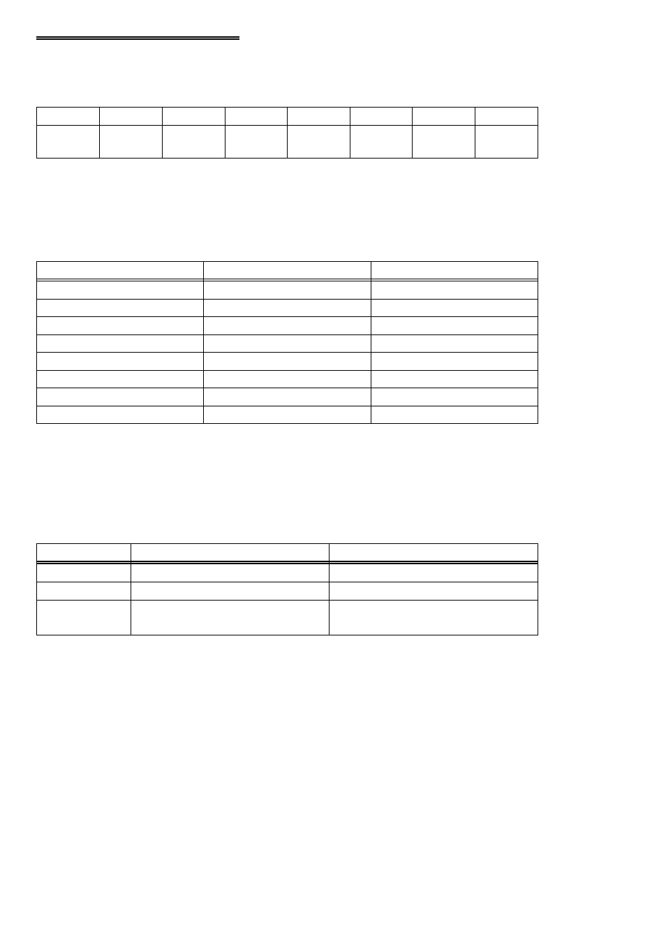
The PPIO-AI08 register descriptions follow the format:
CH1
CH2
CH4
CH8
A/D12
LSB
A/D11
A/D10
A/D9
0
1
2
3
4
5
6
7
Where the numbers along the top row are the bit positions within the 8-bit byte and
the numbers and symbols in the bottom row are the functions associated with that bit.
To write to or read from a register in decimal or
HEX,
the following weights apply:
80
128
7
40
64
6
20
32
5
10
16
4
8
8
3
4
4
2
2
2
1
1
1
0
HEX VALUE
DECIMAL VALUE
BIT POSITION
To write control or data to a register, the individual bits must be set to “0” or “1”, then
combined to form a byte.
The registers and their function are listed on the following table. Each register has
eight bits which can constitute a byte of data or eight individual set/read functions.
OP1 - OP4,
INTE
&
MUX
Address
EOC,
IP1-IP3,
IRQ,
MUX
Address
BASE
+ 2
Start 8 bit A/D conversion
A/D Bits 9-12(LSB)
BASE
+ 1
Start 12 bit A/D conversion
A/D Bits 1(MSB)
−8
BASE
+ 0
WRITE FUNCTION
READ FUNCTION
ADDRESS
8
- ACC-300 (7 pages)
- AI-EXP32 (20 pages)
- AI-EXP48 (19 pages)
- BTH-1208LS (30 pages)
- 6K-ERB08 (32 pages)
- BTH-1208LS Quick Start (4 pages)
- 6K-SSR-RACK08 (33 pages)
- BTH-1208LS-OEM (27 pages)
- CB-COM-Digital (68 pages)
- CB-7018 (68 pages)
- CB-7000 Utilities (44 pages)
- CB-7080D (74 pages)
- CB-COM-7033 (44 pages)
- CB-COM-7017 (72 pages)
- CB-COM-7024 (76 pages)
- CB-NAP-7000P (36 pages)
- CIO-DAC02/16 (16 pages)
- CIO-DAC02 (18 pages)
- CB-NAP-7000D (56 pages)
- CIO-DAC16-I (16 pages)
- CIO-DAC16/16 (20 pages)
- CIO-DAS08 (21 pages)
- CIO-DAC16 (20 pages)
- CIO-DAS08/JR (16 pages)
- CIO-DAS08/JR/16 (14 pages)
- CIO-DAS08/JR-AO (16 pages)
- CIO-DAS08-AOM (32 pages)
- CIO-DAS08-PGM (28 pages)
- CIO-DAS16/330 (34 pages)
- CIO-DAS48-I (17 pages)
- CIO-DAS16/M1 (38 pages)
- CIO-DAS48-PGA (18 pages)
- CIO-DAS800 (20 pages)
- CIO-DAS802/16 (22 pages)
- CIO-DAS6402/16 (40 pages)
- CIO-DAS-TEMP (20 pages)
- CIO-DDA06/16 (18 pages)
- CIO-DDA06/JR (17 pages)
- CIO-DIO24H (20 pages)
- CIO-DIO24/CTR3 (21 pages)
- CIO-DI192 (24 pages)
- CIO-DDA06 (21 pages)
- CIO-DIO48 (19 pages)
- CIO-DO192H (16 pages)
- CIO-DIO192 (20 pages)