Digital input/output – Measurement Computing USB-2408 Series User Manual
Page 28
USB-2408 Series User's Guide
Specifications
28
Digital input/output
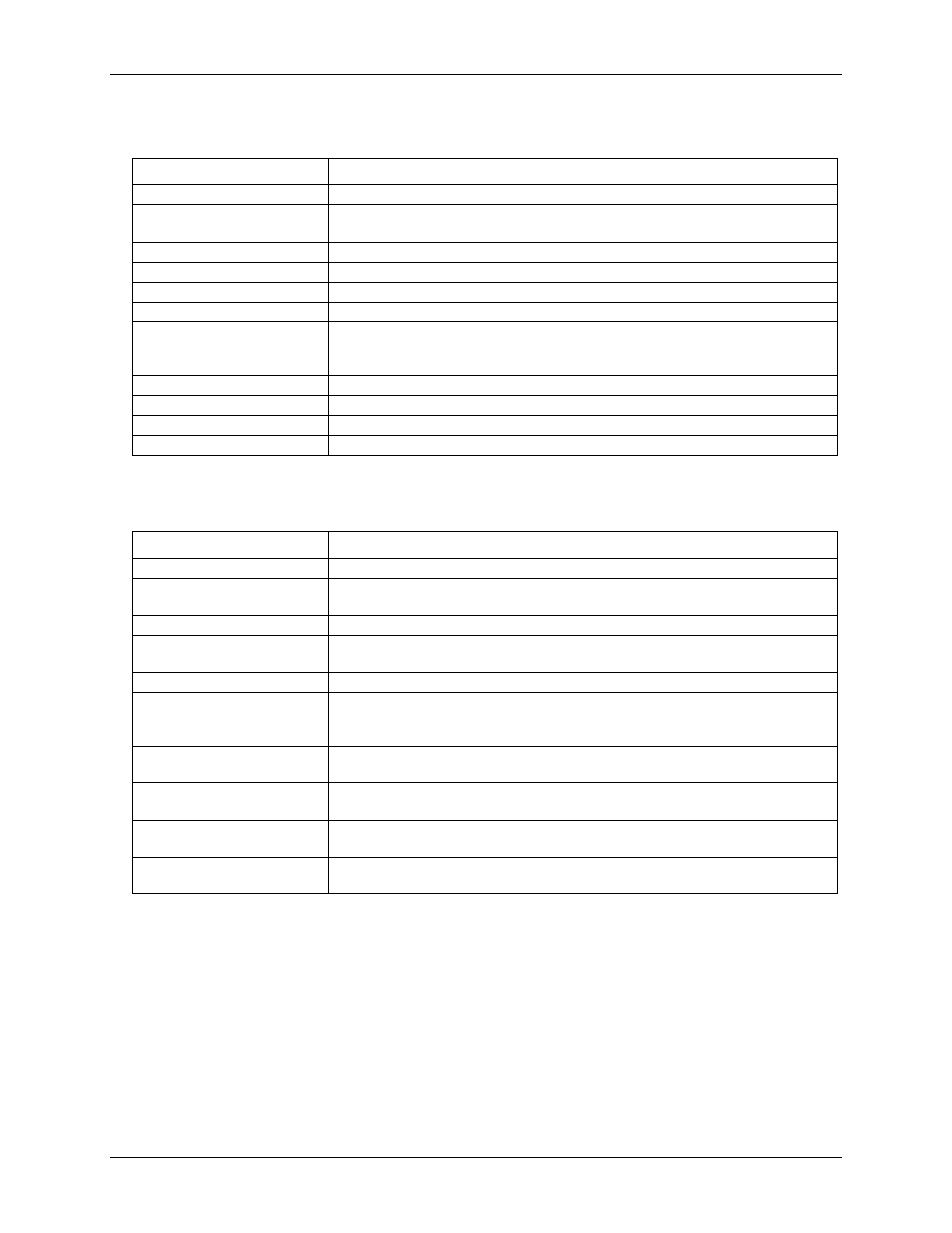
Table 18. Digital input specifications
Parameter
Specifications
Number of I/O
8 channels
Configuration
Each DIO bit can be independently read from (DIN) or written to (DOUT).
The DIN bits can be read at any time whether the DOUT is active or tri-stated.
Input voltage range
0 to +15 V
Input type
CMOS (Schmitt trigger)
Input characteristics
47 kΩ pull-up/pull-down resistor, 28 kΩ series resistor
Maximum input voltage range
0 V to +20 V max (power on/off, relative to DGND) (Note 2)
Pull-up/pull-down
configuration
All pins pulled up to +5 V via individual 47 kΩ resistors (the J6 shorting block default
position is pins 1 and 2).
Pull down capability is available by placing the J6 shorting block across pins 2 and 3.
Transfer rate (software paced)
500 port reads or single bit reads per second typ.
Input high voltage
1.3 V min, 2.2 V max
Input low voltage
1.5 V max, 0.6 V min
Schmitt trigger hysteresis
0.4 V min, 1.2 V max
Note 2:
DGND pins are recommended for use with digital input and digital output pins. The DGND and
AGND pins are common and are isolated from earth ground.
Table 19. Digital output specifications
Parameter
Specifications
Number of I/O
8 channels
Configuration (Note3)
Each DIO bit can be independently read from (DIN) or written to (DOUT).
The DIN bits may be read at any time whether the DOUT is active or tri-stated
Output characteristics (Note 4)
47 kΩ pull-up, open drain (DMOS transistor)
Pull-up configuration
All pins pulled up to +5 V via individual 47 kΩ resistors (the J6 shorting block default
position is pins 1 and 2).
Transfer rate (software paced)
Digital output – 500 port writes or single-bit writes per second typ.
Output voltage range
0 V to +5 V (no external pull up resistor, internal 47 kΩ pull-up resistors connected to
+5 V by default)
0 V to +15 V max (Note 5)
Drain to source breakdown
voltage
+50 V min
Off state leakage current
(Note 6)
1.0 µA
Sink current capability
150 mA max (continuous) per output pin
150 mA max (continuous) for all eight channels
DMOS transistor on-resistance
(drain to source)
4 Ω
Note 3:
DGND pins are recommended for use with digital input and digital output pins. The DGND and
AGND pins are common and are isolated from earth ground.
Note 4:
Each DMOS transistor source pin is internally connected to DGND.
Note 5:
The external pull-up is connected to the digital output bit through an external pull-up resistor. Adding
an external pull-up resistor connects it in parallel with the internal 47 kΩ pull-up resistor of that
particular digital input/output bit. Careful consideration should be made when considering the external
pull-up resistor value and the resultant pull-up voltage produced at the load.
Note 6:
Does not include the additional leakage current contribution that may occur when using an external
pull-up resistor.