Introducing the pci-dda02/12, Functional block diagram – Measurement Computing PCI-DDA02/12 User Manual
Page 5
5
Chapter 1
Introducing the PCI-DDA02/12
The PCI-DDA02/12 provides two channels of 12-bit analog output and 48-bits of digital I/O.
The D/A converters can be independently configured for either Bipolar or Unipolar. Bipolar ranges are ±10 V,
±5 V, and ±2.5 V. Unipolar ranges are 0 to 10 V, 0 to 5 V, and 0 to 2.5 V. The outputs may be updated
individually or simultaneously. The range settings are software-selectable.
The digital I/O ports are configured as two 82C55 mode 0 emulations. Each group is divided into three 8-bit
ports — Port A, Port B, and Port C. Port C can be split into two four-bit ports — Port C-HI and Port C-LO.
Each of these ports may be individually programmed as input or output. The digital outputs are capable of
sinking 64 mA and sourcing 15 mA utilizing standard "S" logic.
The PCI interface uses the PLX 9052 chip, which is a slave-only device. The PCI interface for the analog output
is configured in a 16-bit, multiplexed address/data bus, I/O access mode. The PCI interface for the digital I/O is
configured in an 8-bit, multiplexed address/data bus, I/O access mode to be register-compatible with the PCI-
DIO48H and PCI-DIO96H boards.
The PCI-DDA02/12 board is completely plug-and-play, with no jumpers or switches to set. All board addresses
are set by the board's plug-and-play software. Board configuration is controlled by your system's BIOS.
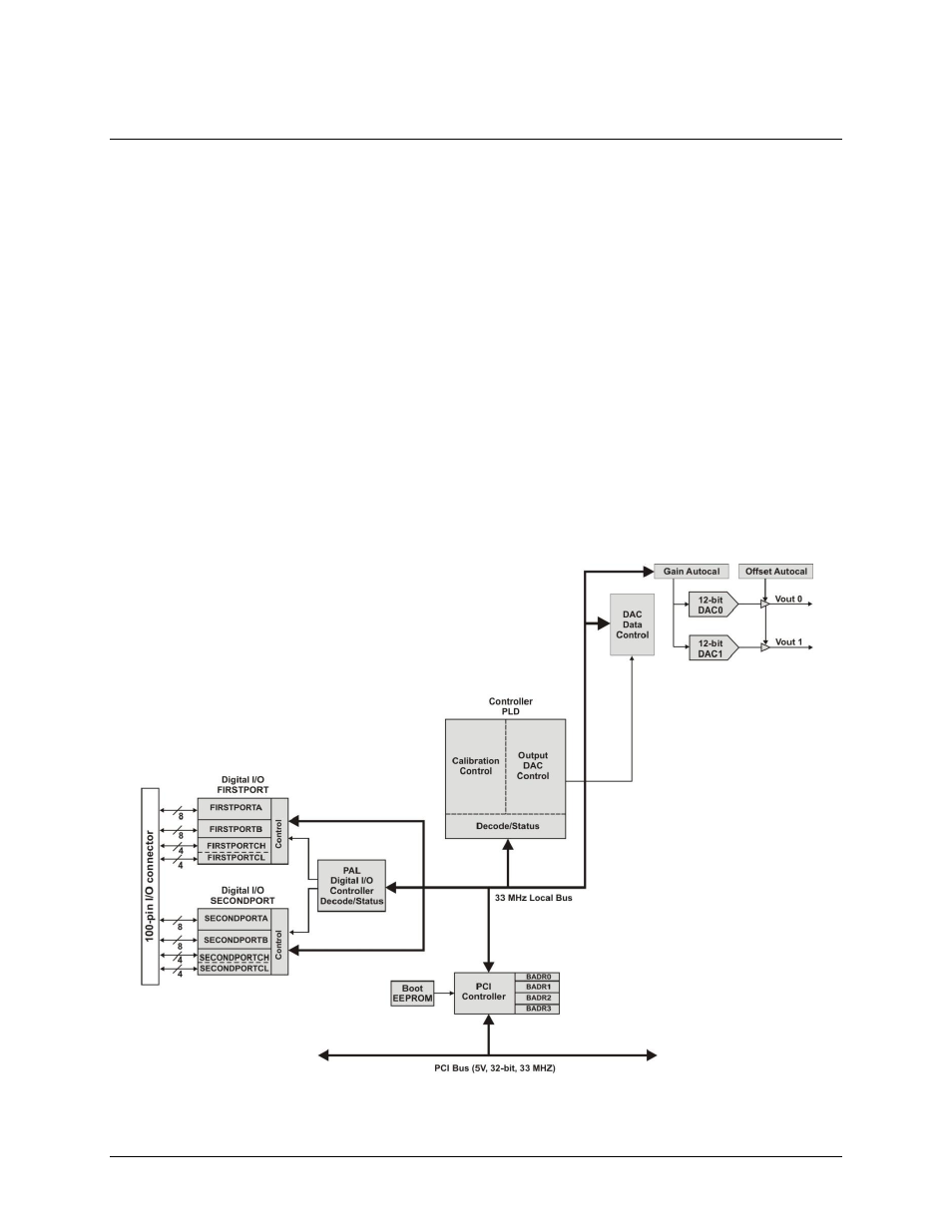
Functional block diagram
PCI-DDA02/12 functions are illustrated in the block diagram shown here.
Figure 1. PCI-DDA02/12 functional block diagram