Functional details, Pci-das-tc block diagram, Chapter 3 – Measurement Computing PCI-DAS-TC User Manual
Page 12: Plx9050 pci interface
12
Chapter 3
Functional Details
PCI-DAS-TC Block diagram
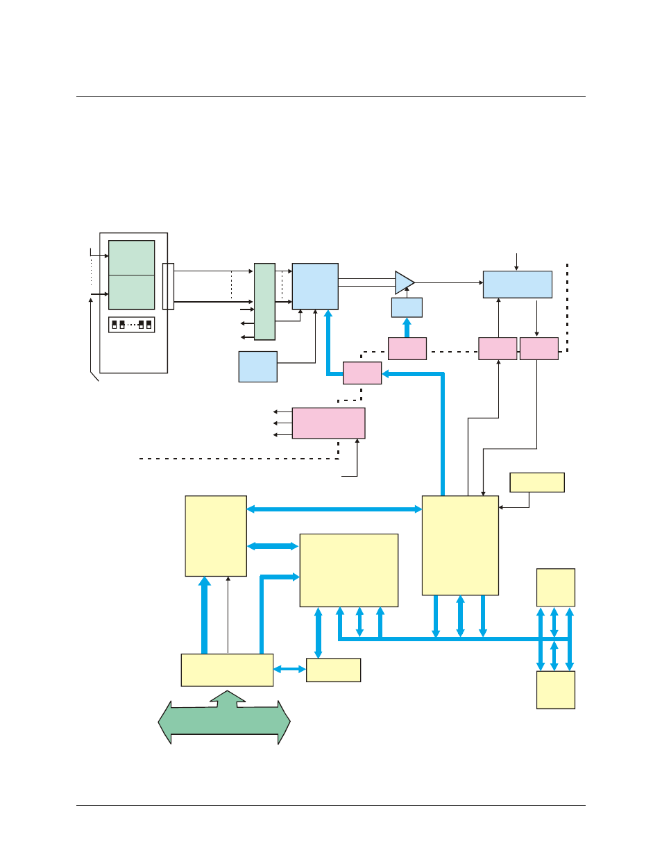
PCI-DAS-TC functions are illustrated in the block diagram shown here.
Dual Port
SRAM
AM188
CPU
Control
Logic
Control
Registers
Flash
EPROM
Local BUS - Address, Data, Control
Programmable
Logic
Data
D0:7
Board
Select
Processing and Control Section
Oscillator
System +5
Isolation
Barrier
DC/DC
Converter
SELECT:
CJC
Gain
Channel
Calibration
Fout
CLK
IN
V/F
Converter
+10V Ref
Gain
Mux
Input AMP
20
Channel
Mux
37
Pin
+10V
Prec.
Ref
+5V ISO
+15V ISO
-15V ISO
Input
Connector
+9.9V
CJC
AGND
TC Input
Channels
0 - 15
Screw
Terminal
CJC
Open
Thermocouple
Detection
Switches
0
15
External
DAS-TC
Screw Terminal
(For CJC) +15ISO
Thermocouple
Input
Channels
Isolated Analog Input Section
32-BIT, 33 MHz, 5V PCI BUS
PLX9050
PCI Interface
Control
Signals
Local
Control
Address
Data Bus
Transceiver
SRAM
Optical
Isolator
Optical
Isolator
Optical
Isolator
Optical
Isolator
Figure 3. PCI-DAS-TC functional block diagram
- ACC-300 (7 pages)
- AI-EXP32 (20 pages)
- AI-EXP48 (19 pages)
- BTH-1208LS (30 pages)
- 6K-ERB08 (32 pages)
- BTH-1208LS Quick Start (4 pages)
- 6K-SSR-RACK08 (33 pages)
- BTH-1208LS-OEM (27 pages)
- CB-COM-Digital (68 pages)
- CB-7018 (68 pages)
- CB-7000 Utilities (44 pages)
- CB-7080D (74 pages)
- CB-COM-7033 (44 pages)
- CB-COM-7017 (72 pages)
- CB-COM-7024 (76 pages)
- CB-NAP-7000P (36 pages)
- CIO-DAC02/16 (16 pages)
- CIO-DAC02 (18 pages)
- CB-NAP-7000D (56 pages)
- CIO-DAC16-I (16 pages)
- CIO-DAC16/16 (20 pages)
- CIO-DAS08 (21 pages)
- CIO-DAC16 (20 pages)
- CIO-DAS08/JR (16 pages)
- CIO-DAS08/JR/16 (14 pages)
- CIO-DAS08/JR-AO (16 pages)
- CIO-DAS08-AOM (32 pages)
- CIO-DAS08-PGM (28 pages)
- CIO-DAS16/330 (34 pages)
- CIO-DAS48-I (17 pages)
- CIO-DAS16/M1 (38 pages)
- CIO-DAS48-PGA (18 pages)
- CIO-DAS800 (20 pages)
- CIO-DAS802/16 (22 pages)
- CIO-DAS6402/16 (40 pages)
- CIO-DAS-TEMP (20 pages)
- CIO-DDA06/16 (18 pages)
- CIO-DDA06/JR (17 pages)
- CIO-DIO24H (20 pages)
- CIO-DIO24/CTR3 (21 pages)
- CIO-DI192 (24 pages)
- CIO-DDA06 (21 pages)
- CIO-DIO48 (19 pages)
- CIO-DO192H (16 pages)
- CIO-DIO192 (20 pages)