Analog output, Accuracy, Analog output drift – Measurement Computing PCI-DAS1602/16 User Manual
Page 24
PCI-DAS1602/16 User's Guide
Specifications
23
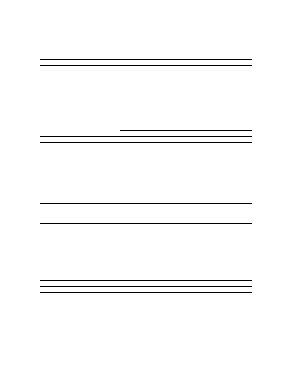
Analog output
Table 6. Analog output specifications
D/A converter type
AD669BR
Resolution
16 bits
Number of channels
2
Channel type
Single-ended voltage output
Output range (each channel independently
software selectable)
±10 V, ±5 V, 0 to 10 V, or 0 to 5 V
Data transfer
From 512 sample FIFO via REPOUTSW or programmed I/O. Data
interleaved for dual analog output mode.
Throughput
100 kHz, 2 channels simultaneous
Monotonicity
16 bits at 25 °C
Slew rate
10 V ranges: 6 V/µs
5 V ranges: 3 V/µs
Settling time
13 µS max 20 V step to 0.0008%
6 µS typ 10V step to 0.0008%
Current drive
±5 mA min
Output short-circuit duration
Indefinite @ 25 mA
Output coupling
DC
Output impedance
0.1 ohms max
Output stability
Any passive load
Coding
Offset binary
Output voltage on power up and reset
0 V ± 10 mV
Accuracy
Table 7. Analog output accuracy specifications
Range
Accuracy
BIP10
±8 LSB
BIP5
±8 LSB
UNI10
±10 LSB
UNI5
±10 LSB
Accuracy Components
Integral linearity error
±0.5 LSB typ, ±1 LSB max
Differential linearity error
±0.5 LSB typ, ±1 LSB max
Analog output drift
Table 8. Analog output drift specifications
Analog output full-scale gain drift
±0.22 LSB/°C max
Analog output zero drift
±0.22 LSB/°C max
Overall analog output drift
±0.44 LSB/°C max
Absolute error change per °C temperature change is a combination of the gain and offset drift of many
components. The theoretical worst case error of the board may be calculated by summing these component
errors. Worst case error is realized only in the unlikely event that each of the component errors is at their
maximum level, and causing error in the same direction.