Analog output, Absolute accuracy, Calibrated accuracy components – Measurement Computing PCI-DAS1002 User Manual
Page 20
PCI-DAS1002 User's Manual
Specifications
20
Analog output
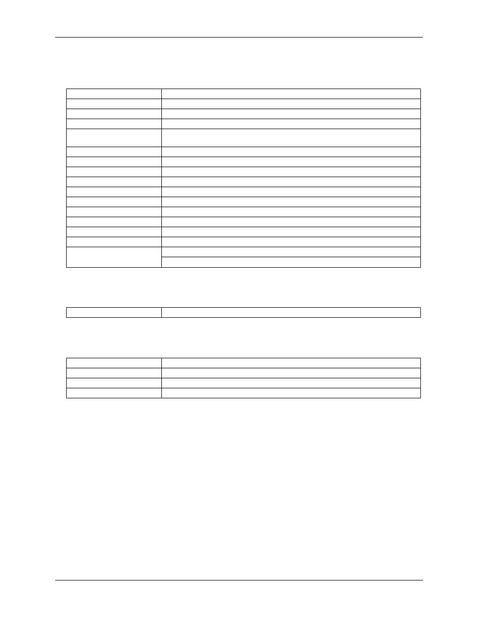
Table 6. Analog output specifications
D/A converter type
AD7847AR or equivalent
Resolution
12 bits
Number of channels
2
Configuration
Voltage output, single-ended
Output range
±10 V, ±5 V, 0 to 10 V, or 0 to 5 V. Software selectable. Each channel independently
programmable.
D/A pacing
Software
Data transfer
Programmed I/O
Monotonicity
Guaranteed monotonic over temperature
Overall analog output drift
±0.03 LSB/°C max
Settling time
4 µs to 0.01% of 10 V step
Slew rate
7 V/µs min
Current drive
±5 mA min
Output short-circuit duration
Indefinite @25 mA
Output coupling
DC
Output impedance
0.1 Ohm, max
Miscellaneous
Double buffered output latches
Output voltage on power up and reset: ±200 mV
Absolute accuracy
Table 7. Absolute accuracy specifications (analog output)
All ranges
±3 LSB
Calibrated accuracy components
Table 8. Calibrated accuracy specifications (analog output)
Gain error
±1.0 LSB max
Offset error
±0.5LSB max
Integral linearity error
±1.0 LSB max
Differential linearity error
±1.0 LSB max
Each PCI-DAS1002 is tested at the factory to assure absolute accuracy.
Total analog output error is a combination of gain, offset, integral linearity and differential linearity error. The
theoretical worst-case error of the board may be calculated by summing these component errors. Worst case
error is realized only in the unlikely event that each of the component errors are at their maximum level, and
causing error in the same direction. Although an examination of the chart and a summation of the maximum
theoretical errors shows that the board could theoretically exhibit a ±3.5 LSB error, our testing assures this error
is never realized in a board that we ship.