Accuracy, Crosstalk, Noise performance – Measurement Computing PCI-DAS1002 User Manual
Page 19
PCI-DAS1002 User's Manual
Specifications
19
Accuracy
Accuracies are listed for a 200 kHz sampling rate, 100 sample average, single channel operation, a 15 minute
warm-up, and operational temperatures within ±2 C of internal calibration temperature. The calibrator test
source high side is tied to Channel 0 In and the low side is tied to AGND.
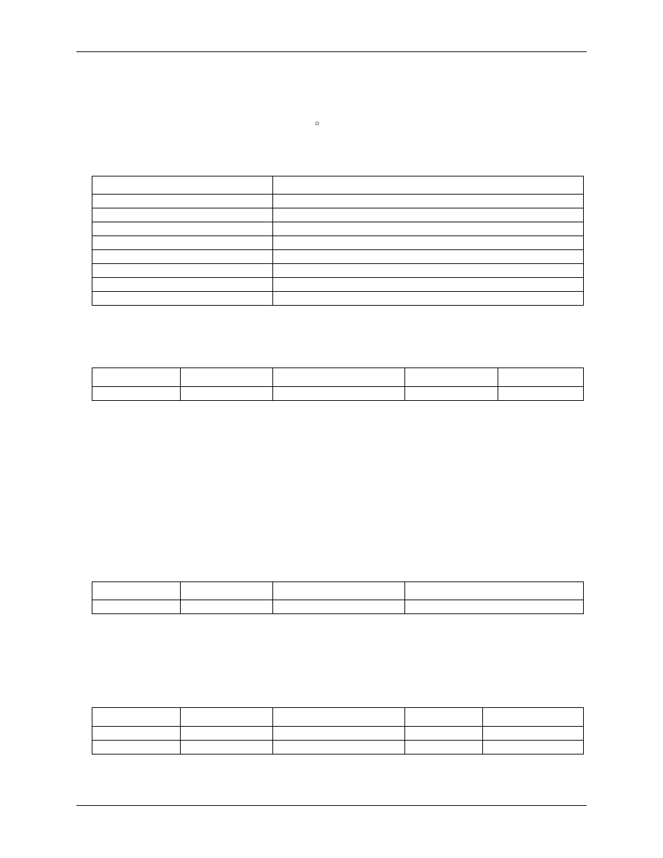
Table 2. Absolute accuracy specifications (analog input)
Range
Absolute Accuracy
±10.00 V
±2.5 LSB max
±5.000 V
±2.5 LSB max
±2.500 V
±2.5 LSB max
±1.250 V
±2.5 LSB max
0 to 10.00 V
±2.5 LSB max
0 to 5.000 V
±2.5 LSB max
0 to 2.500 V
±2.5 LSB max
0 to 1.250 V
±2.5 LSB max
Each PCI-DAS1002 is tested at the factory to assure the board’s overall error does not exceed accuracy limits
described in Table 2 above.
Table 3. Calibrated accuracy components (in LSB)
Range
Gain Error
Offset Error
DLE
ILE
All ranges
±1.0 max
±1.0 max
±0.75 max
±0.5 max
As shown in Table 3, total board error is a combination of gain, offset, differential linearity and integral
linearity error. The theoretical worst-case error of the board may be calculated by summing these component
errors. Worst case errors are realized only in the unlikely event that each of the component errors are at their
maximum level, and causing error in the same direction.
Crosstalk
Crosstalk is defined here as the influence of one channel upon another when scanning two channels at the
maximum rate. A full scale 100 Hz triangle wave is input on channel 1; Channel 0 is tied to analog ground at
the 100-pin user connector. The table below summarizes the influence of channel 1 on channel 0 with the
effects of noise removed. The residue on channel zero is described in LSB’s.
Table 4. Crosstalk specifications
Condition
Crosstalk
Per channel Rate
ADC Rate
All ranges
2 LSB
pk-pk
100 kHz
200 kHz
Noise performance
Table 5 below summarizes the noise performance for the PCI-DAS1002. Noise distribution is determined by
gathering 50 K samples at 200 kHz with inputs tied to ground at the user connector.
Table 5. Board noise performance
Range
% within ±2 LSB
% within ±1 LSB
LSBs
LSBrms*
0 to 1.250 V
100%
99%
4
0.61
All other ranges
100%
100%
3
0.45
* RMS noise is defined as the peak-to-peak bin spread divided by 6.6.