Pci-das08 block diagram, Pci-das08 block diagram -2, Pci-das08 user's guide introducing the pci-das08 – Measurement Computing PCI-DAS08 User Manual
Page 8: Figure 1-1. pci-das08 block diagram
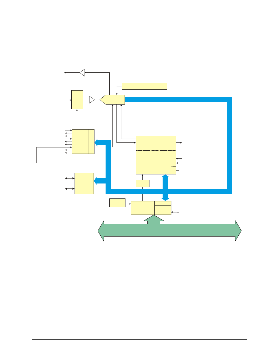
PCI-DAS08 User's Guide
Introducing the PCI-DAS08
PCI-DAS08 block diagram
PCI-DAS08 functions are illustrated in the block diagram shown here.
PCI
Controller
BADR1
Interrupt
Boot
EEPROM
Counter 2
Clock
(33 MHz/8)
Interrupt
Control
Decode/Status
Bus
Timing
Channel Select
Output Clock2
EXT_INT
Controller FPGA and Logic
LOCAL BUS
PCI BUS (5 V, 32-BIT, 33 MHZ)
Input
Port
C
ont
ro
l
Input (2:0)
Digital I/O
82C54
16-bit Counters
Input Clock2
Counter 0
Co
n
tr
o
l
Counter 1
Counter 2
Input Clock0
Gate0
Output Clock0
Input Clock1
Gate1
Output Clock1
Gate2
Output Clock2
Output
Port
Output (3:0)
ADC and MUX
Control
10 Volt
Reference
Channel Select
Gain and Offset Cal
Mux
Analog In
8 CH S.E.
Buffer
12-bit, 100 kHz
Start EOC
Buffer
BADR2
A/D
Control
Figure 1-1. PCI-DAS08 block diagram
1-2
See also other documents in the category Measurement Computing Hardware:
- ACC-300 (7 pages)
- AI-EXP32 (20 pages)
- AI-EXP48 (19 pages)
- BTH-1208LS (30 pages)
- 6K-ERB08 (32 pages)
- BTH-1208LS Quick Start (4 pages)
- 6K-SSR-RACK08 (33 pages)
- BTH-1208LS-OEM (27 pages)
- CB-COM-Digital (68 pages)
- CB-7018 (68 pages)
- CB-7000 Utilities (44 pages)
- CB-7080D (74 pages)
- CB-COM-7033 (44 pages)
- CB-COM-7017 (72 pages)
- CB-COM-7024 (76 pages)
- CB-NAP-7000P (36 pages)
- CIO-DAC02/16 (16 pages)
- CIO-DAC02 (18 pages)
- CB-NAP-7000D (56 pages)
- CIO-DAC16-I (16 pages)
- CIO-DAC16/16 (20 pages)
- CIO-DAS08 (21 pages)
- CIO-DAC16 (20 pages)
- CIO-DAS08/JR (16 pages)
- CIO-DAS08/JR/16 (14 pages)
- CIO-DAS08/JR-AO (16 pages)
- CIO-DAS08-AOM (32 pages)
- CIO-DAS08-PGM (28 pages)
- CIO-DAS16/330 (34 pages)
- CIO-DAS48-I (17 pages)
- CIO-DAS16/M1 (38 pages)
- CIO-DAS48-PGA (18 pages)
- CIO-DAS800 (20 pages)
- CIO-DAS802/16 (22 pages)
- CIO-DAS6402/16 (40 pages)
- CIO-DAS-TEMP (20 pages)
- CIO-DDA06/16 (18 pages)
- CIO-DDA06/JR (17 pages)
- CIO-DIO24H (20 pages)
- CIO-DIO24/CTR3 (21 pages)
- CIO-DI192 (24 pages)
- CIO-DDA06 (21 pages)
- CIO-DIO48 (19 pages)
- CIO-DO192H (16 pages)
- CIO-DIO192 (20 pages)