Pci-dac6702 and pci-dac6703 block diagram, Software features – Measurement Computing PCI-DAC6702 User Manual
Page 9
PCI-DAC6702 and PCI-DAC6703 User's Guide
Introducing the PCI-DAC6702 and PCI-DAC6703
9
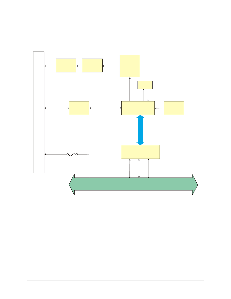
PCI-DAC6702 and PCI-DAC6703 block diagram
PCI-DAC6702 and PCI-DAC6703 board functions are illustrated in the block diagram shown here.
Bus Interface
Logic
+5V
1
0
0
-P
in
I
/O
C
o
n
n
e
c
to
r
0.75 A
Resettable
circuit breaker
D
a
ta
A
d
d
re
s
s
C
o
n
tr
o
l
L
O
C
A
L
B
U
S
Temperature
Sensor
Digital I/O
8-bit
Control
Voltage
Output
Circuit
Main
Voltage
Circuit
16-Bit
DAC
DIO (7:0)
RAM
Data
nvRAM
PCI BUS (5V, 32-Bit, 33MHZ)
RAM
Address/
Control
DAC
Out
PCI-DAC6703 x 16
PCI-DAC6702 x 8
Figure 1. PCI-DAC6702 and PCI-DAC6703 functional block diagram
Software features
For information on the features of InstaCal and the other software included with your PCI-DAC6702 and PCI-
DAC6703, refer to the Quick Start Guide that shipped with your device. The Quick Start Guide is also available
in PDF
Check
for the latest software version or versions of the software supported
under less commonly used operating systems.