Analog output calibration, Digital input / output, Power consumption – Measurement Computing PCI-DAC6702 User Manual
Page 19: Environmental, Mechanical
PCI-DAC6702 and PCI-DAC6703 User's Guide
Specifications
19
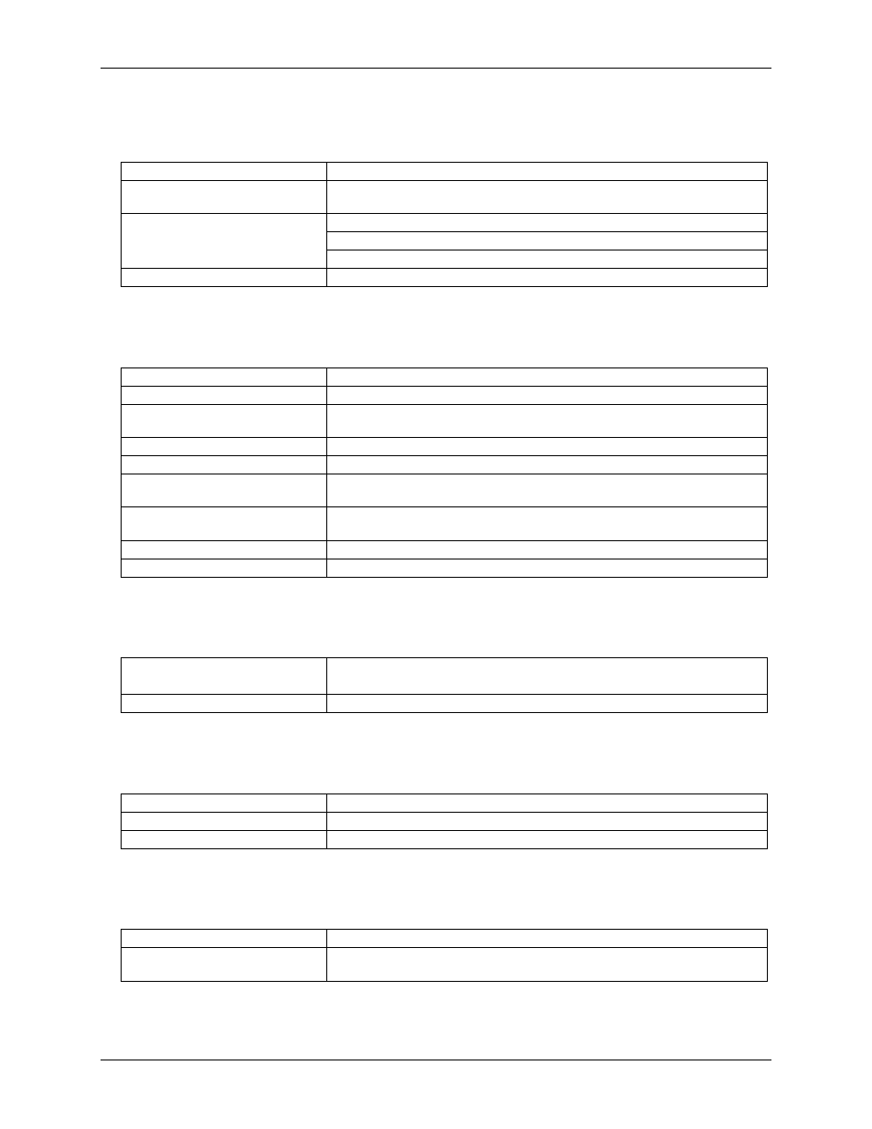
Analog output calibration
Table 5. Analog I/O calibration
Recommended warm-up time
15 minutes
Calibration
Auto-calibration, calibration factors for each range stored on board in non-volatile
RAM.
Onboard calibration reference
DC Level: 10.000 V± 1 mV. Actual measured values stored in EEPROM.
Tempco: 0.6 ppm/°C max
Long-term stability: ±6 ppm/sqrt(1000 hrs)
Calibration interval
1 year
Digital input / output
Table 6. Digital I/O
Digital type
Discrete, 5 V/TTL compatible
Number of I/O
8
Configuration
8 bits, independently programmable for input or output. Position available for
pull-up/pull-down resistor network (not populated).
Input high voltage
2.0 V min, 7.0 V absolute max
Input low voltage
0.8 V max, –0.5 V absolute min
Output high voltage
(IOH = –32 mA)
3.80 V min, 4.20 V typ
Output low voltage
(IOL = 32 mA)
0.55 V max, 0.22 V typ
Data transfer
Programmed I/O
Power-up / reset state
Input mode (high impedance)
Power consumption
Table 7. Power consumption specifications
+5 V
PCI-DAC6703:
1.1 A max
PCI-DAC6702:
1.0 A max
+5 V available at I/O connector
0.75A max, protected with a resettable fuse
Environmental
Table 8. Environmental specifications
Operating temperature range
0 to 55 °C
Storage temperature range
-20 to 70 °C
Humidity
0 to 90% non-condensing
Mechanical
Table 9. Mechanical specifications
Card dimensions
PCI half card: 174.4 mm (L) x 106.9 mm (W) x18.4 mm (H)
Form factor
Universal PCI keying. Compatible with either 3.3 V or 5 V PCI signaling
environments.