Specifications, Analog output, Chapter 4 – Measurement Computing PCI-DAC6702 User Manual
Page 18
18
Chapter 4
Specifications
Typical for 25 °C unless otherwise specified.
Specifications in italic text are guaranteed by design
Analog output
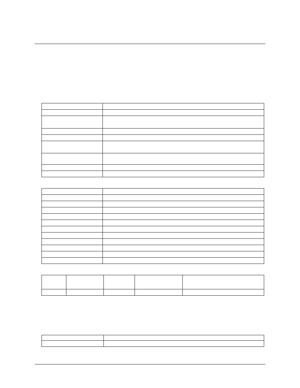
Table 1. Analog output specifications
D/A converter type
Enhanced R-2R
Resolution
16-bits, 1 in 65536
Number of channels
PCI-DAC6703:
16 voltage
PCI-DAC6702:
8 voltage
DNL
±1 LSB max
Monotonicity
16-bits, guaranteed after calibration
Update rate, max
PCI-DAC6703:
1111 S/s per channel
PCI-DAC6702:
1111 S/s per channel
Update modes
Software selectable per channel for update immediate (default), or update from
NVRAM on command
Output short-circuit duration
Indefinite @ 25 mA
Power-on state
Independent, user-defined power-on states.
Table 2. Voltage output specifications
Range
±10.1 V
Output coupling
DC
Output impedance
0.1 Ω max.
Current drive
±10 mA max
Load capacitance
10,000 pF
Slew rate
0.5 V/µs typ.
Settling time (full scale step)
7.2 ms max to ±0.5 LSB
Noise
100 µVrms, DC to 1 MHz BW
Offset temperature coefficient
±5 µV/ºC
Gain temperature coefficient
±1 ppm/ºC
Protection
Short circuit to ground
Data transfer
Programmed I/O
Table 3. Absolute accuracy components - all values are (±)
Range
1
% of Reading
Offset
Temp Drift
2
(%/ºC)
Absolute Accuracy at FS
±10 V
0.0019
±710 µV
0.0001
±1 mV
Note 1:
Temp drift applies only if the ambient temperature changes by more than ±10ºC since the last
calibration.
Note 2:
Each PCI-DAC670x board is tested at the factory to assure that the overall error does not exceed
the values specified in Table 3.
Table 4. Relative accuracy
Range
Relative Accuracy
±10 V
±1.0 LSB, max
Relative accuracy is defined as the measured deviation from a straight line drawn between measured endpoints
of the transfer function.