Figure 3-10 – Measurement Computing miniLAB-1008 User Manual
Page 23
miniLAB 1008 User's Guide
Functional
Details
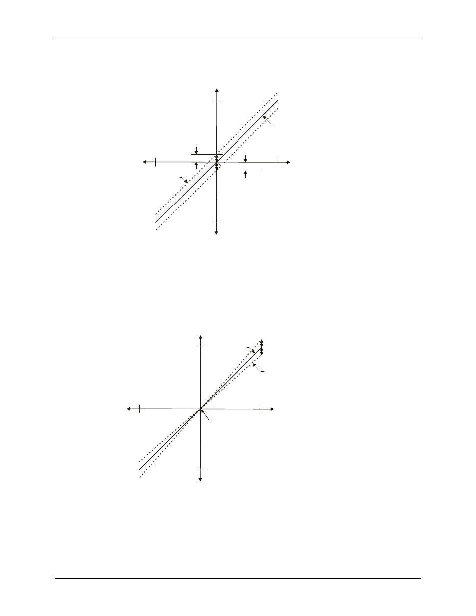
The accuracy plots in Figure 3-10 are drawn for clarity and are not drawn to scale.
-FS
+FS
Input Voltage
0
4095
2
Offset=9.77mV
Ideal
Actual
Output Code
9.77mV
2048
Figure 3-10. ADC transfer function with offset error
Gain error is a change in the slope of the transfer function from the ideal, and is typically expressed as a
percentage of full-scale.
shows the miniLAB 1008 transfer function with gain error. Gain error is
easily converted to voltage by multiplying the full-scale (FS) input by the error.
Figure 3-11. ADC Transfer function with gain error
The accuracy plots in Figure 3-11 are drawn for clarity and are not drawn to scale.
-FS
+FS
Input Voltage
0
4095
Actual
Ideal
Output Code
Gain error=+0.2%, or +20 mV
Gain error=-0.2%, or -20 mV
2048
For example, the miniLAB 1008 exhibits a typical calibrated gain error of ±0.2% on all ranges. For the ±10 V
range, this would yield 10V × ±0.002 = ±20 mV. This means that at full scale, neglecting the effect of offset for
the moment, the measurement would be within 20 mV of the actual value. Note that gain error is expressed as a
ratio. Values near ±FS are more affected from an absolute voltage standpoint than are values near mid-scale,
which see little or no voltage error.
3-11