Aplex Technology ACS-2685 User Manual
Page 26
ACS-2685 User Manual
26
LB_D2_P
22
21
LA_D2_P
Ground
24
23
Ground
LB_CLK_N
26
25
LA_CLK_N
LB_CLK_P
28
27
LA_CLK_P
Ground
30
29
Ground
LVDS_DDC_DATA
32
31
LVDS_DOC_CLK
Ground
34
33
Ground
LB_D3_N
36
35
LA_D3_N
LB_D3_P
38
37
LA_D3_P
NC
40
39
NC
14. BT1:
POWER on/off Button, They are used to connect power switch button. The two pins
are disconnected under normal condition. You may short them temporarily
to realize system startup & shutdown or awaken the system from sleep
state.
15. JCOM1:
(2.0mm Pitch 2x3 Pin Header),COM1 jumper setting, pin 1~6 are used to select
signal out of pin 9 of COM1 port.
JP3 Pin#
Function
Close 1-2 COM1 RI (Ring Indicator)
(default)
Close 3-4
COM1 Pin9=+5V
(option)
Close 5-6
COM1 Pin9=+12V
(option)
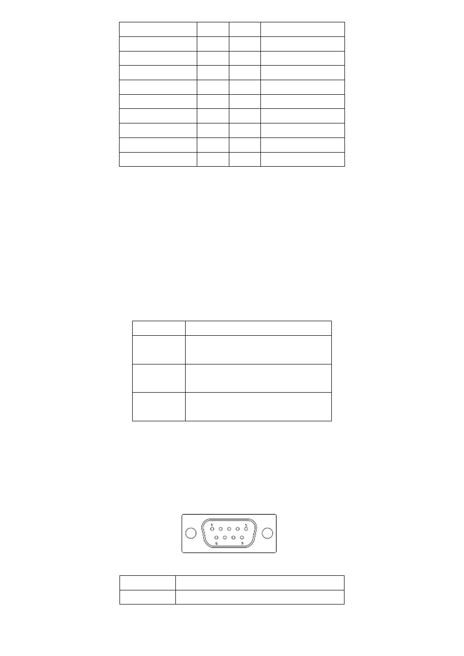
16. COM1:
(Type DB9),Rear serial port, standard DB9 Male serial port is provided to make a
direct connection to serial devices. COM1 port is controlled by pins No.1~6 of
JCOM1,select output Signal RI or 5V or 12v, For details, please refer to description of
JCOM1.
Pin#
Signal Name
1
DCD# (Data Carrier Detect)