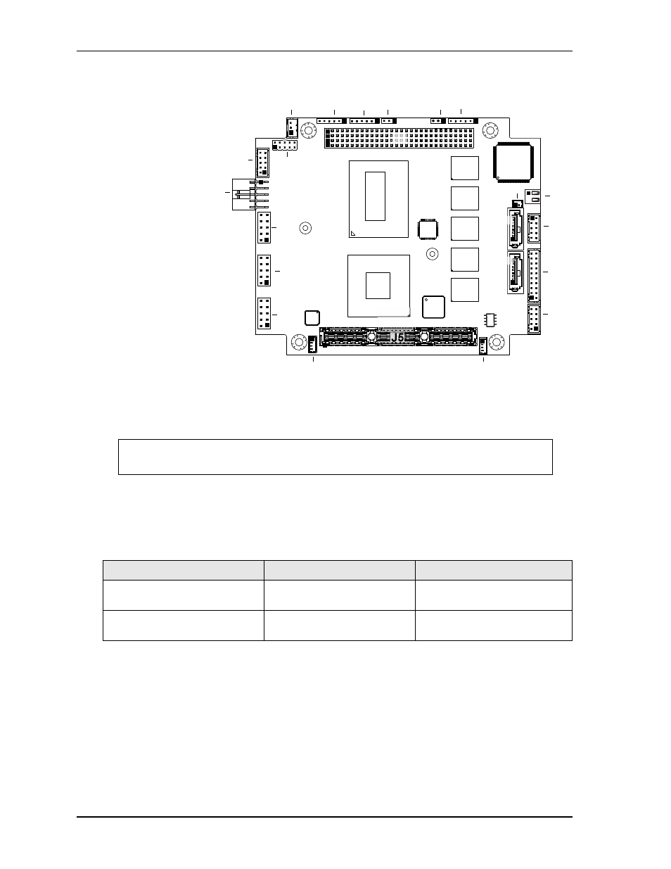
Figure 2-6, Jumper header definitions, Header, connector, and socket locations (top side) – ADLINK CoreModule 920 User Manual
Page 22: Table 2-3, Jumper settings

Chapter 2
Product Overview
16
Reference Manual
CoreModule 920
Figure 2-6. Header, Connector, and Socket Locations (Top Side)
Jumper Header Definitions
describes the jumper headers shown in
. Both jumper headers provide 0.079" (2mm)
pitch.
NOTE
Black square pins on headers and connectors represent pin 1. Black square pins on
right-angle headers represent pin 2.
Table 2-3. Jumper Settings
Jumper Header
Installed
Moved
JP1 – LVDS Voltage Selection
(HIROSE, A4B-3PA-2DSA)
Enable +3.3V (1-2) (Default)
Enable +5V (2-3)
JP2 – PCI-104 Voltage Selection
(HIROSE, A4B-3PA-2DSA)
Enable +3.3V (1-2) (Default)
Enable +5V (2-3)
CM920_T
op_Conn_b
Key:
H11 - GLAN1
H15 - USB 0-1
H16 - COM2
J2 - LED, GLAN1 (PHY Transceiver)
J3 - LED, GLAN2 (Gb Controller)
J5 - PCIe/104
J6 - PCIe/104 (see Bottom Component View)
J7 - PCI-104
J8 - HDMI (Micro)
J10 - SATA0
J12 - Battery
J13 - SATA1
J14 - GLAN2
J17 - VGA
J18 - COM1
J21 - Utility
J22 - Fan
J23 - LVDS
J24 - Power
J25 - USB 2-3
J26 - GPIO 5-8
J27 - GPIO 1-4
JP1 - LVDS Voltage (see jumper table)
JP2 - PCI-104 Voltage (see jumper table)
SW1 - PCIe x16 Configuration Switch (see Bottom Component View)
J26
J14
J3
J2
H11
H15
H16
J24
J25
J17
J22
J12
J23
J18
J21
JP1
J8
JP2
J27
J13
J10
J5
J7
