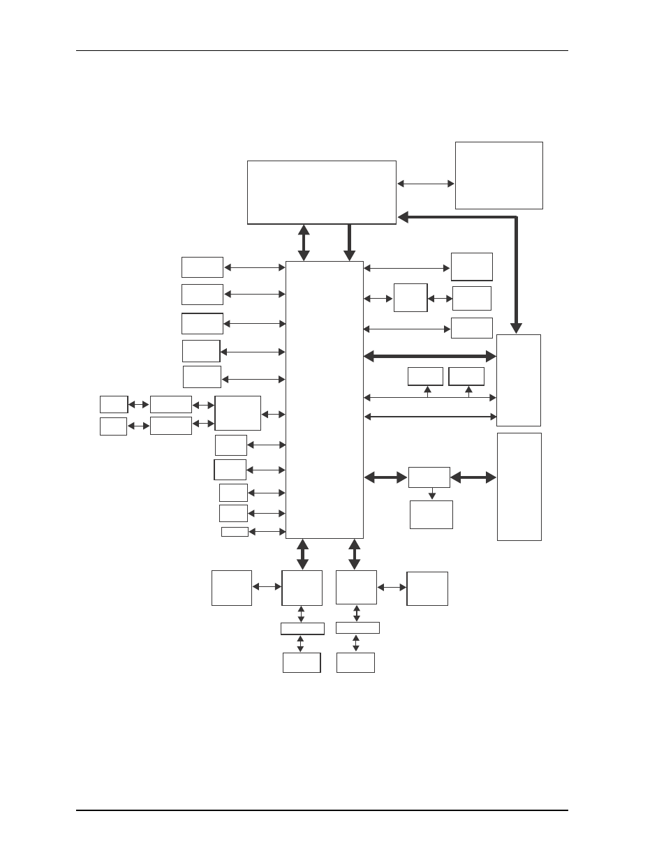
Block diagram, Figure 2-2, Functional block diagram – ADLINK CoreModule 920 User Manual
Page 16: Figure 2-2. functional block diagram

Chapter 2
Product Overview
10
Reference Manual
CoreModule 920
Block Diagram
presents a functional representation of the CoreModule 920.
Figure 2-2. Functional Block Diagram
FDI
DMI
1333MHz,
1.5V, 2GB
PCH
Intel
BD82QM67
Intel
82574IT
MAC & PHY
Controller
USB 0-1
Header
USB 2-3
Header
PCIe x1
PCIe x1, Lanes 1-4
PCIe x1
SATA 3.0, Port 0
SATA 3.0, Port 1
SATA 2.0, Port 2
32-bit PCI
33 MHz
COM1
COM2
SPI
BIOS
VGA
VGA
Header
HDMI
Connector
PCI-104
Connector
HDMI
Level
Shifter
HDMI
TMDS
24-bit LVDS
LVDS
Header
SATA0
Connector
SATA1
Connector
SSD
PCIe-to-PCI
Bridge
PCIe/104
Connector
GPIO
GPIO
Header
GPIO
GPIO
Header
LPC
Serial
Header
RS232
Transceiver
RS232
Transceiver
Serial
Header
LPC to UART
Controller
F81216
SMBus
USB 2.0, Ports 4-5
USB 2.0, Ports 0-1
USB 2.0, Ports 2-3
VBAT
CPLD
Battery
Header
Utility
Header
Intel
82579LM
PHY
Transceiver
GLAN1
LED
Header
GLAN2
LED
Header
GLAN1
Header
Transformer
Transformer
PCIe x1
GLAN2
Header
CM920_blk_diag_a
CPU
Intel
Core i7 3517UE (Dual-Core) 1.7GHz (17W)
(with integrated Processor Core
and Graphics Memory Hub)
PCIe x16 Graphics (1) [PEG],
1x16; 2x8; 1x8 & 2x4
Memory Bus
8x DDR3 SDRAM
System Memory
(2Gb each)
1x DDR3 SDRAM
System Memory (ECC)
(2Gb each)
Hardware
Monitor
SPD
EEPROM
PCIe-to-PCI
Bridge
EEPROM
