Figure 2-5, Connector pin sequence – ADLINK CoreModule 920 User Manual
Page 21

Chapter 2
Product Overview
CoreModule 920
Reference Manual
15
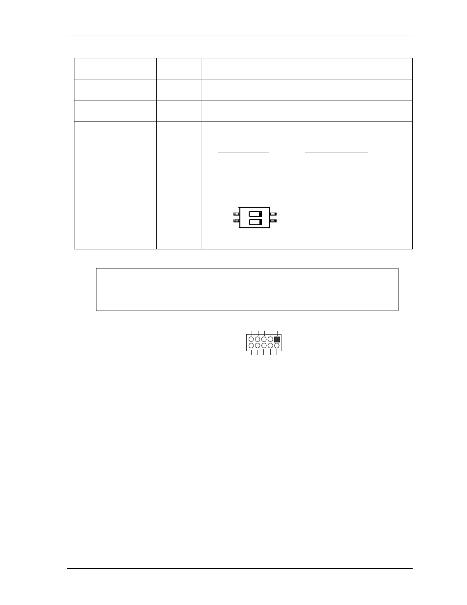
Figure 2-5. Connector Pin Sequence
J25 – USB 2-3
Top
10-pin, 0.079" (2mm) shrouded header for USB 2.0 ports 2-3
(HIROSE, DF11-10DP-2DSA)
J26 – GPIO1
Top
6-pin, 0.079" (2mm) single-row header for GPIO1
(SAMTEC, TMM-106-03-L-S)
J27 – GPIO2
Top
6-pin, 0.079" (2mm) single-row header for GPIO2
(SAMTEC, TMM-106-03-L-S)
SW1 – PCIe x16 Lane
Configuration Switch
(see
Bottom
4-pin dip switch for selecting CPU PCIe x16 lane configurations
(WIN WIN, DHN-02-T-V-T/R)
Switch Positions Lane Configurations
1-OFF, 2-OFF = 1x16 [Default]
1-OFF, 2-ON = 2x8
1-ON, 2-OFF = Reserved
1-ON, 2-ON = 1x8, 2x4
NOTE
The pinout tables in Chapter 3 of this manual identify pin sequence using the
following method: A 10-pin header with two rows of pins, using odd/even
numbering, where pin 2 is directly across from pin 1, is noted as 10-pin, 2 rows, odd/
even (1, 2). See
Table 2-2. Module Header and Connector Descriptions (Continued)
ON
1 2
(OFF)
(ON)
Switch Positions
1
2
3
4
5
6
7
8
9
10
10-pin, two rows,
Odd/Even, (1, 2)
CM920_ConNum_a
