Pci express™ system management bus (smbus) gpio, Table 3-4, Smbus reserved addresses – ADLINK Express-HRR User Manual
Page 28: Table 3-5, Com express a-b connector signal descriptions
Chapter 3
Hardware
24
Reference Manual
Express-HRR
PCI Express
™
The Express-HRR offers six (6) PCI Express x1 ports (ports 1-6) through the COM Express A-B connector
and two PCI Express x1 ports (ports 7-8) through the C-D connector. These ports can be configured to
support PCI Express edge cards or ExpressCards. Each x1 port supports up to 5 GT/s bandwidth in each
direction. Ports 1-4 and ports 5-8 can be independently configured as four x1s, two x2s, one x2 and two x1s,
or one x4 port widths. The eighth x1 port (port 8) is utilized by the onboard Gigabit Ethernet transceiver and
is unavailable as a PCIe port. The PCI Express interface is based on the PCI Express Specification 2.0.
System Management Bus (SMBus)
The I/O Hub (PCH) contains an integrated SMBus controller with both a host and slave SMBus port; but the
host cannot access the slave internally. The slave port allows an external master access to the PCH through
the COM Express A-B connector.
lists the device names and corresponding reserved addresses on
the SMBus.
GPIO
The Express-HRR provides GPIO (General Purpose I/O) pins for custom use through the COM Express A-
B connector. Use the ADLINK Intelligent Device Interface (AIDI) Library to configure the GPIO interface.
AIDI driver information is available on the COM Express Product page at:
http://www.adlinktech.com
. An
AIDI demo program and the AIDI User’s Manual describing how to use the GPIO pins also reside in the
Utilities areas of the COM Express Product page.
For more information about GPIO pin operation, refer to the Intel 6 Series Chipset Datasheet for the PCH
(BD82QM67) controller. Refer to
for a hyper link to the datasheet.
provides the pin signals for the COM Express A-B connector.
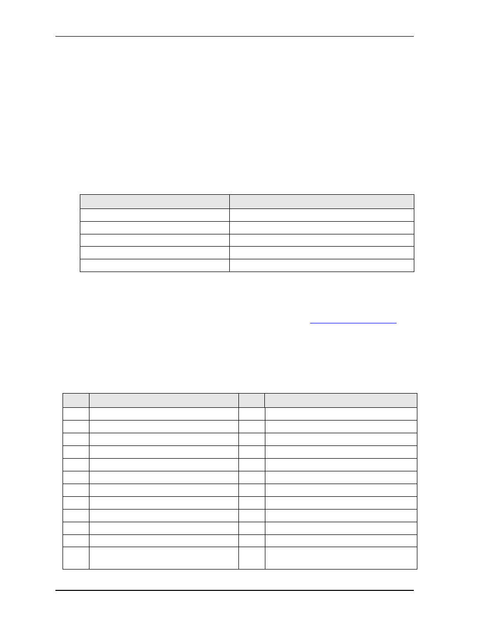
Table 3-4. SMBus Reserved Addresses
Component
Address (hex)
SODIMM A
A0h
SODIMM B
A4h
Hardware Temp and Voltage Monitor
2Eh
GPIO Generator
40h
Clock Generator
D2h
Table 3-5. COM Express A-B Connector Signal Descriptions
Pin #
Row A
Pin #
Row B
A1
GND
B1
GND
A2
GBE0_MDI3-
B2
GBE0_ACT# (PU 10k 3.3V)
A3
GBE0_MDI3+
B3
LPC_FRAME#
A4
GBE0_LINK100# (Ethernet Speed LED)
B4
LPC_AD0
A5
GBE0_LINK1000# (Ethernet Speed LED)
B5
LPC_AD1
A6
GBE0_MDI2-
B6
LPC_AD2
A7
GBE0_MDI2+
B7
LPC_AD3
A8
GBE0_LINK#
B8
LPC_DRQ0# (Int. PU 20k in PCH)
A9
GBE0_MDI1-
B9
LPC_DRQ1# (Int. PU 20k in PCH)
A10
GBE0_MDI1+
B10
LPC_CLK
A11
GND
B11
GND
A12
GBE0_MDI0-
B12
PWRBTN# (PU 10k 3.3V S5
Standby)