Ab signal descriptions, Audio signals, Analog vga – ADLINK Express-IB User Manual
Page 17: Lvds
Express-IB
Page 17
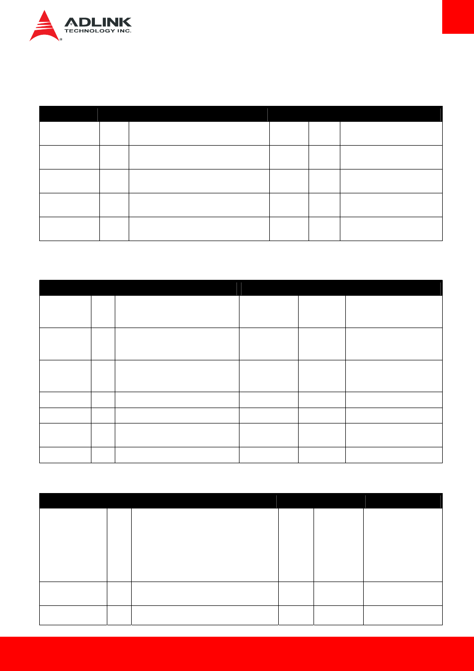
3.3. AB Signal Descriptions
3.3.1. Audio Signals
Signal
Pin #
Description
I/O
PU/PD
Comment
AC_RST# /
HDA_RST#
A30
Reset output to CODEC, active low.
O 3.3VSB
AC_SYNC /
HDA_SYNC
A29
Sample-synchronization signal to the CODEC(s).
O 3.3V
AC_BITCLK /
HDA_BITCLK
A32
Serial data clock generated by the external
CODEC(s).
I/O 3.3V
AC _SDOUT /
HDA_SDOUT
A33
Serial TDM data output to the CODEC.
O 3.3V
AC _SDIN[2:0]
HDA_SDIN[2:0]
B28
B30
Serial TDM data inputs from up to 3 CODECs.
I/O 3.3VSB
3.3.2. Analog VGA
Signal
Pin # Description
I/O
PU/PD
Comment
VGA_RED
B89
Red for monitor.
Analog DAC output, designed to drive a
37.5-Ohm equivalent load.
O Analog
If VGA is used than signal should
be pulled to GND by 150Ω on the
carrier
VGA_GRN
B91
Green for monitor
Analog DAC output, designed to drive a
37.5-Ohm equivalent load.
O Analog
If VGA is used than signal should
be pulled to GND by 150Ω on the
carrier
VGA_BLU
B92
Blue for monitor.
Analog DAC output, designed to drive a
37.5-Ohm equivalent load.
O Analog
If VGA is used than signal should
be pulled to GND by 150Ω on the
carrier
VGA_HSYNC
B93
Horizontal sync output to VGA monitor
O 3.3V
VGA_VSYNC
B94
Vertical sync output to VGA monitor
O 3.3V
VGA_I2C_CK
B95
DDC clock line (I²C port dedicated to identify
VGA monitor capabilities)
I/O OD 3.3V
PU 2k2 3.3V
VGA_I2C_DAT
B96
DDC data line.
I/O OD 3.3V
PU 2k2 3.3V
3.3.3. LVDS
Signal
Pin #
Description
I/O
PU/PD
Comment
LVDS_A0+
LVDS_A0-
LVDS_A1+
LVDS_A1-
LVDS_A2+
LVDS_A2-
LVDS_A3+
LVDS_A3-
A71
A72
A73
A74
A75
A76
A78
A79
LVDS Channel A differential pairs
O LVDS
LVDS_A_CK+
LVDS_A_CK-
A81
A82
LVDS Channel A differential clock
O LVDS
LVDS_B0+
LVDS_B0-
B71
B72
LVDS Channel B differential pairs
O LVDS