17 power and system management, 18 power and ground – ADLINK Express-HL User Manual
Page 24
Page 24
Express-HL
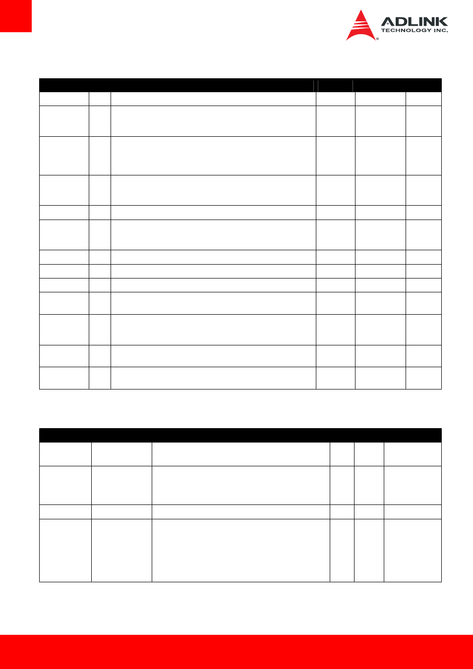
3.3.17 Power And System Management
Signal
Pin # Description
I/O
PU/PD
Comment
PWRBTN#
B12
Power button to bring system out of S5 (soft off), active on falling edge.
I 3.3VSB
PU 10k 3.3VSB
SYS_RESET#
B49
Reset button input. Active low request for module to reset and reboot. May
be falling edge sensitive. For situations when SYS_RESET# is not able to
reestablish control of the system, PWR_OK or a power cycle may be used.
I 3.3V
PU 10k 3.3V
CB_RESET#
B50
Reset output from module to Carrier Board. Active low. Issued by module
chipset and may result from a low SYS_RESET# input, a low PWR_OK
input, a VCC_12V power input that falls below the minimum specification, a
watchdog timeout, or may be initiated by the module software.
O 3.3V
PU 1k 3.3V
PWR_OK
B24
Power OK from main power supply. A high value indicates that the power is
good. This signal can be used to hold off Module startup to allow carrier
based FPGAs or other configurable devices time to be programmed.
I 3.3V
PU 100k
3.3VSB
Should
have weak
pull up
SUS_STAT#
B18
Indicates imminent suspend operation; used to notify LPC devices.
O 3.3VSB
SUS_S3#
A15
Indicates system is in Suspend to RAM state. Active-low output. An inverted
copy of SUS_S3# on the carrier board (also known as “PS_ON”) may be
used to enable the non-standby power on a typical ATX power supply.
O 3.3VSB
SUS_S4# A18
Indicates
system is in Suspend to Disk state. Active low output.
O 3.3VSB
SUS_S5#
A24
Indicates system is in Soft Off state.
O 3.3VSB
WAKE0#
B66
PCI Express wake up signal.
I 3.3VSB
PU 10k 3.3VSB
WAKE1#
B67
General purpose wake up signal. May be used to implement wake-up on
PS/2 keyboard or mouse activity.
I 3.3VSB
PU 10k 3.3VSB
BATLOW#
A27
Battery low input. This signal may be driven low by external circuitry to
signal that the system battery is low, or may be used to signal some other
external power-management event.
I 3.3VSB
PU 8.2k 3.3VSB
LID#
A103 LID button. Low active signal used by the ACPI operating system for a LID
switch.
I OD
3.3VSB
PU 10k 3.3VSB
SLEEP#
B103 Sleep button. Low active signal used by the ACPI operating system to bring
the system to sleep state or to wake it up again.
I OD
3.3VSB
PU 10K 3.3VSB
3.3.18 Power and Ground
Signal
Pin #
Description
I/O
PU/PD
Comment
VCC_12V A104-A109
B104-B109
Primary power input: +12V nominal (8.5 ~ 20V wide input).
All available VCC_12V pins on the connector(s) shall be used.
P
8.5~20
V
VCC_5V_SBY
B84-B87
Standby power input: +5.0V nominal. If VCC5_SBY is used, all
available VCC_5V_SBY pins on the connector(s) shall be used.
Only used for standby and suspend functions. May be left
unconnected if these functions are not used in the system design.
P
5Vsb
±5%
VCC_RTC
A47
Real-time clock circuit-power input. Nominally +3.0V.
P
GND
A1, A11, A21, A31,
A41, A51, A57, A66,
A80, A90, A96,
A100, A110, B1,
B11, B21 ,B31, B41,
B51, B60, B70, B80,
B90, B100, B110
Ground - DC power and signal and AC signal return path.
P