9 switch and jumper settings, Clear cmos switch (sw4), Vga/gpio mode switches (sw1, sw3) – ADLINK cPCI-3615 User Manual
Page 55: Switch and jumper settings, Table 4-19: vga/gpio
Board Interfaces
41
cPCI-3615
4.9
Switch and Jumper Settings
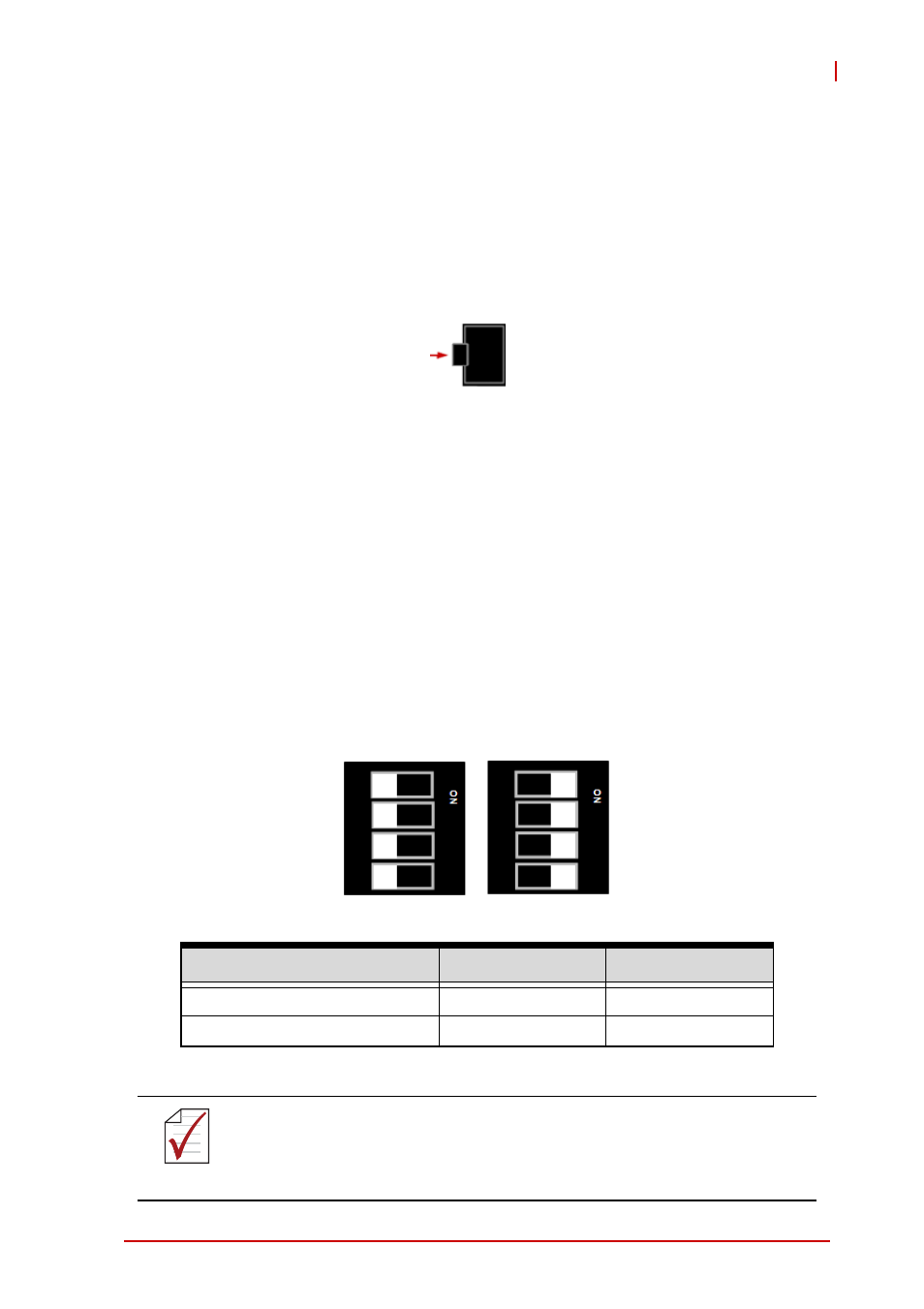
Clear CMOS Switch (SW4)
The cPCI-3615 comes with a Clear CMOS switch to reset the
CMOS values to default. The switch is located on solder side of
the board, under the "CE" logo. Press the switch to clear the
CMOS and reset the values to default.
VGA/GPIO Mode Switches (SW1, SW3)
The VGA and GPIO 4~7 signals to J2 share the same pins and
are selected by switch settings. SW1 is located on the
cPCI-3615 component side (see “cPCI-3615 Blade Board Lay-
out” on page 19 and “Removing the DB-3610CF Daughter
Board” on page 59) and SW3 is located on the solder side
behind SW1. When the switches are set to VGA mode, the
VGA signals are available to J2, and there are only four GPIO
signals connected to J2 (GPIO 0~3). When the switches are
set to GPIO mode, there are eight GPIO signals connected to
J2 and VGA output to the RTM is not available. The switches
are set to VGA mode by default.
Table 4-19: VGA/GPIO Mode Switch Settings
Mode
SW1
SW3
VGA (default)
All OFF
All ON
GPIO 4~7
All ON
All OFF
NOTE:
NOTE:
To enable VGA output on the RTM, Onboard VGA Output Select
must be set to Rear in the BIOS Advanced Chipset Settings.
SW1
SW3