6 adc timing control, 1 timebase architecture, 2 basic acquisition timing – ADLINK PCIe-9814 User Manual
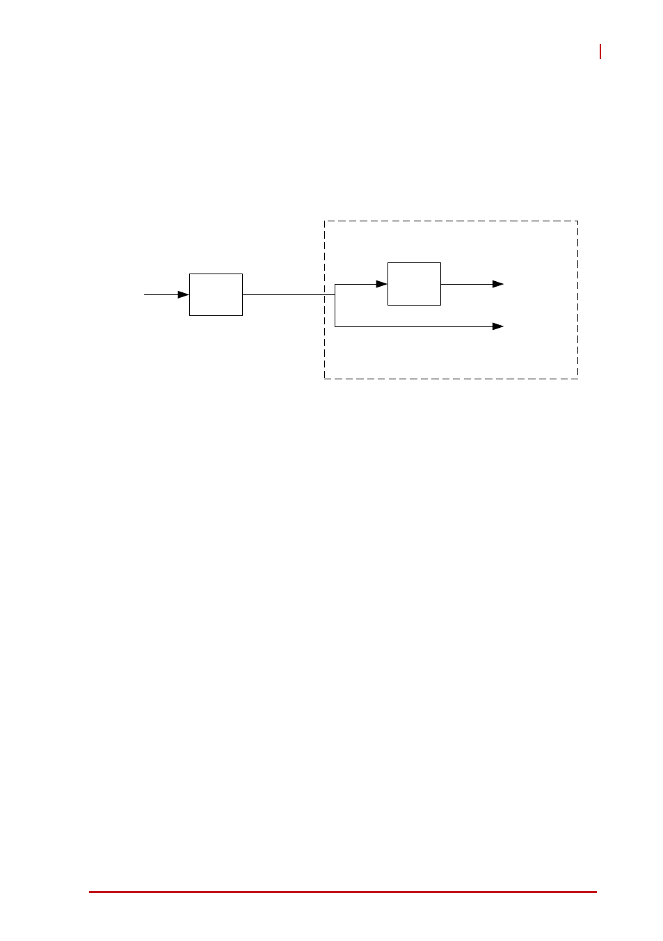
Page 33: Adc timing control, Timebase architecture, Basic acquisition timing, Figure 3-12, Pcie-9814 timebase architecture

Operations
23
PCIe-9814
For more information, refer to the WD-DASK Function Library Ref-
erence.
3.6 ADC Timing Control
3.6.1
Timebase Architecture
Figure 3-12: PCIe-9814 Timebase Architecture
3.6.2
Basic Acquisition Timing
The PCIe-9814 commences acquisition upon receipt of a trigger
event originating with software command, external digital trigger.
The Timebase is a clock provided to the ADC and acquisition
engine for essential timing. The Timebase is from an onboard syn-
thesizer. To achieve different sampling rates, a scan interval coun-
ter is used.
Using the post-trigger mode as an example, as shown, when a
trigger is accepted by the digitizer, the acquisition engine com-
mences acquisition of data from ADC, and stores the sampled
data to the onboard FIFO. When FIFO is not empty, data will be
transferred to system memory immediately through the DMA
engine. The sampled data is generated continuously at the rising
edge of Timebase according to the scan interval counter setting.
When sampled data reaches a specified value, in this example
256, acquisition ends.
ADC
X6
Multiplier
PLL
For ADC
State machine
For ADC
Data Bus
80MHz
480MHz
FPGA
ADC Output
80MHz
Onboard
80MHz
Oscillator
