2 input range and data format, Input range and data format – ADLINK PCIe-9814 User Manual
Page 24

14
Operations
not only accurate DC performance but also high signal-to-noise
ratio, and high spurious-free dynamic range in AC perfor-
mance. The ADC transfers data to system memory via the high
speed PCI Express Gen 1 X 4 interface.
For auto-calibration, internal calibration provides stable and
accurate reference voltage to the AI.
3.2.2
Input Range and Data Format
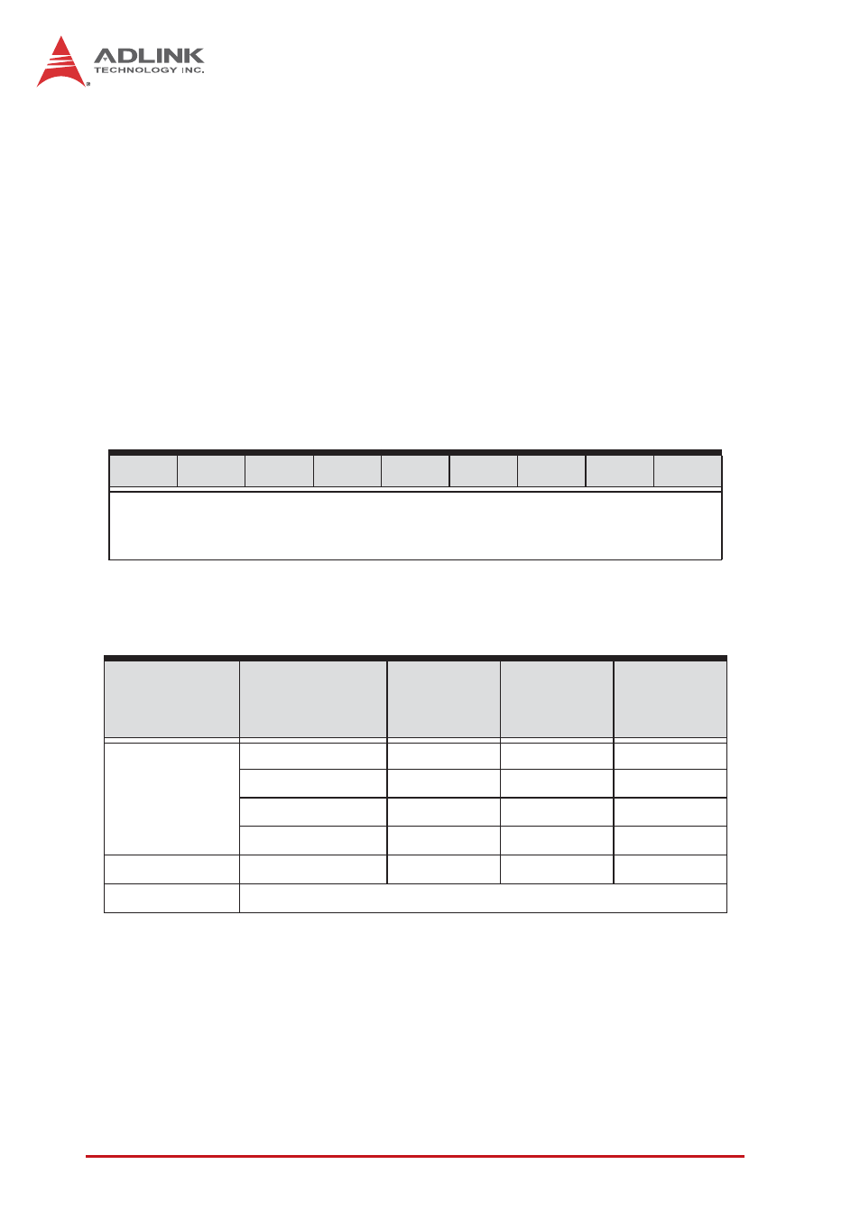
Data format of the PCIe-9814 is 2’s complement. The ADC data of
PCIe-9814 is on the 12 MSB of the 16-bit A/D data. D2 to D0 is
SDI2 to SDI0, with D3 disregarded. A/D data structure is as fol-
lows.
Table 3-1: Input Range and Data Format
Table 3-2: Input Range FSR and –FSR Values
D15
D14
D13
D12
….
D3
D2
D1
D0
D15 to D4 bits represent the data from ADC (2’s complement)
D2 is SDI2, D1 SDI1, D0 SDI0, and D3 is disregarded
Description
Full scale
range
Least
significant
bit
FSR-1LSB
-FSR
Bipolar Analog
Input
±10V
4.88mV
9.9512V
-10V
±5V
2.44mV
4.99756V
-5V
±1V
0.488mV
0.99512V
-1V
±0.5V
0.244mV
0.499756V
-0.5V
Digital Code
N/A
N/A
7FF0
8000
Comment
SDI bit is assumed to be 0
