ADLINK PXIS-2630 Series User Manual
Page 36
30 ● Pin Assignments
4
GND V(I/O)
PXI_BRSVB4
C/BE[7]# GND C/BE[6]#
GND
3
GND
PXI_LBR7 GND PXI_LBR8
PXI_LBR9
PXI_LBR10 GND
2
GND
PXI_LBR11
PXI_LBR12
N/C (SYS#)
PXI_LBL7
PXI_LBL8 GND
1
GND
PXI_LBL9 GND PXI_LBL10
PXI_LBL11
PXI_LBL12 GND
Pin Z
A
B
C
D
E
F
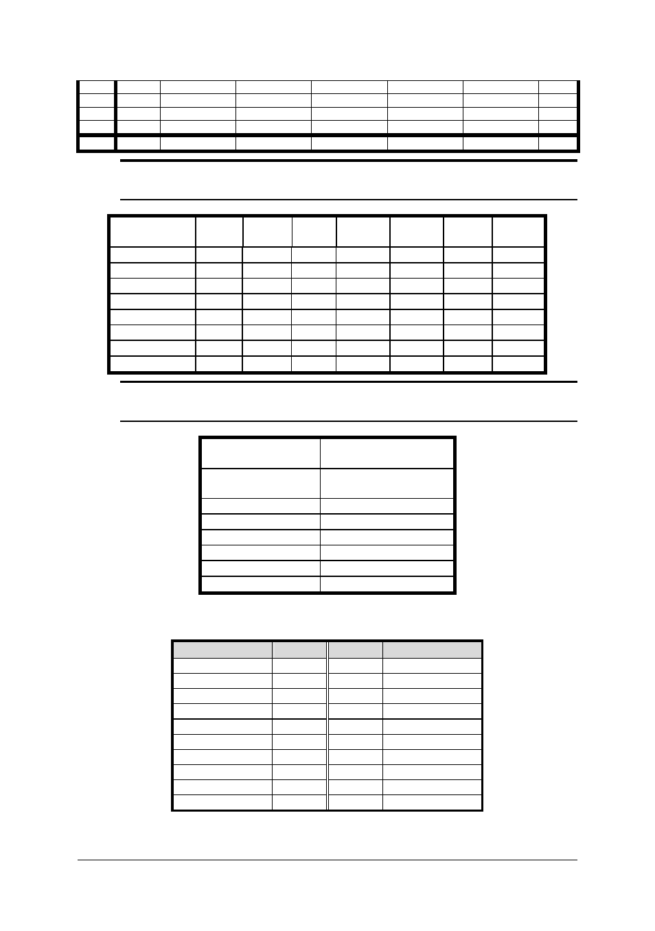
Note 1: Please refer the following table for the routing of the Bus Mastering
(REQ/GNT), IDSEL, PCI CLK, and Interrupt signals.
IDSEL
REQ#
/GNT#
PCI
CLK
PXI P1
Pin A3
PXI P1
Pin B3
PXI P1
Pin C3
PXI P1
Pin E3
Slot 1(SYS)
-
-
-
INTA#
INTB# INTC#
INTD#
Slot 2
AD31
0
6
INTD#
INTA#
INTB#
INTC#
Slot 3
AD30
1
5
INTC#
INTD#
INTA#
INTB#
Slot 4
AD29
2
1
INTB#
INTC#
INTD#
INTA#
Slot 5
AD28
3
2
INTA#
INTB#
INTC#
INTD#
Slot 6
AD27
4
3
INTD#
INTA#
INTB#
INTC#
Slot 7
AD26
5
4
INTC#
INTD#
INTA#
INTB#
Slot 8
AD25
6
0
INTB#
INTC#
INTB#
INTA#
Note 2: Please refer the following table for the routing of the PXI_STAR
addressing signals from the trigger slot to peripheral slots.
Physical Slot
Number
PXI_STAR
(P2-D17)
Slot 2
(Star Trigger Slot)
PXI_STAR0
~ PXI_STAR5
Slot 3
PXI_STAR0
Slot 4
PXI_STAR1
Slot 5
PXI_STAR2
Slot 6
PXI_STAR3
Slot 7
PXI_STAR4
Slot 8
PXI_STAR5
B.2.2 Miscellaneous Connectors Pin Assignments
CN3: ATX-like DC Power input connectors
Signal Name
Pin #
Pin # Signal Name
V2SENSE
1
11
V2 (+3.3V)
V2 (+3.3V)
2
12
V4 (-12V)
GND 3
13 GND
V1 (+5V)
4
14
INH#
GND
5
15
GND
V1 (+5V)
6
16
SRTN
GND 7
17 GND
FAL#1 8*
18*
V3SENSE
DEG#1 9*
19
V1SENSE
V3 (+12V)
10
20
V1 (+5V)