3 external clock mode, External clock mode, Digital input fifo – ADLINK PCIe-7200 User Manual
Page 42
Operation Theory
33
4.3
External Clock Mode
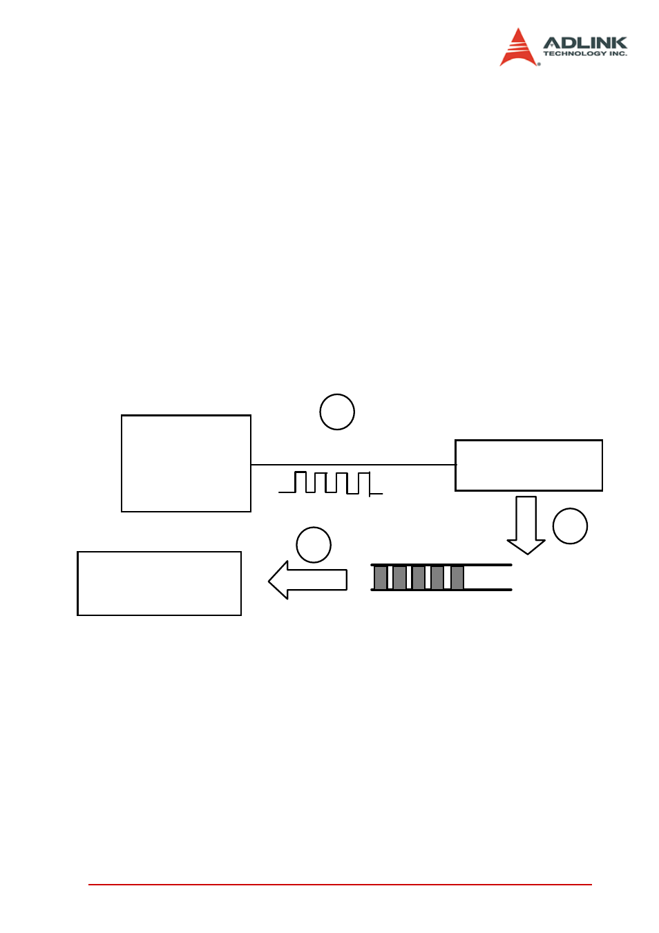
The digital input is clocked by external strobe, which is from Pin 19
(I_REQ) of CN2 (PCI/PCIe-7200) or Pin 24 of CN1 (cPCI-7200).
The operation sequence is very similar to the Timer Pacer Trigger.
The only difference is the clock source.
1. The external input strobe is generated from outside
device, and goes through the Pin 19 (I_REQ) of CN2 to
latch the digital input.
2. The digital input data is saved in FIFO after an I/O strobe
signal is coming in.
3. The data saved in input FIFO will be transferred to main
memory on your computer system directly. This is con-
trolled by bus mastering DMA control, this function is
supported by PCI.
To Digital Input Trigger
Latch Digital
Input Data
Digital Input FIFO
Bus mastering
DMA data Transfer
PC's Main Memory
1
2
3
Pin 19 of CN2
- USB-1901 (84 pages)
- USB-1210 (54 pages)
- USB-2401 (60 pages)
- USB-7230 (50 pages)
- USB-2405 (56 pages)
- DAQe-2010 (92 pages)
- DAQe-2204 (100 pages)
- DAQe-2213 (94 pages)
- DAQe-2501 (74 pages)
- PXI-2010 (84 pages)
- PXI-2020 (60 pages)
- PXI-2501 (62 pages)
- cPCI-9116 (98 pages)
- ACL-8112 Series (93 pages)
- ACL-8112 Series (94 pages)
- ACL-8112 Series (92 pages)
- ACL-8216 (75 pages)
- ACL-8111 (61 pages)
- PCM-9112+ (10 pages)
- PCM-9112+ (94 pages)
- cPCI-6216V (47 pages)
- ACL-6126 (28 pages)
- ACL-6128A (40 pages)
- PCM-6308V+ (52 pages)
- PCM-6308V+ (4 pages)
- PCI-7444 (82 pages)
- PCI-7434 (48 pages)
- PCI-7234 (56 pages)
- PCI-7260 (66 pages)
- PCI-7258 (38 pages)
- PCI-7256 (48 pages)
- PCI-7250 (48 pages)
- LPCI-7250 (48 pages)
- PCI-7396 (65 pages)
- PCI-7296 (59 pages)
- PCI-8554 (67 pages)
- PCIe-7360 (94 pages)
- PCIe-7350 (86 pages)
- PCIe-7300A (114 pages)
- PCI-7300A (112 pages)
- PCI-7300A (83 pages)
- PCI-7200 (96 pages)
- cPCI-7300 (82 pages)
- cPCI-7300 (83 pages)