6 connector pin assignment, Installation • 15 – ADLINK PCI-7224 User Manual
Page 23
Installation
• 15
2.6 Connector
Pin
Assignment
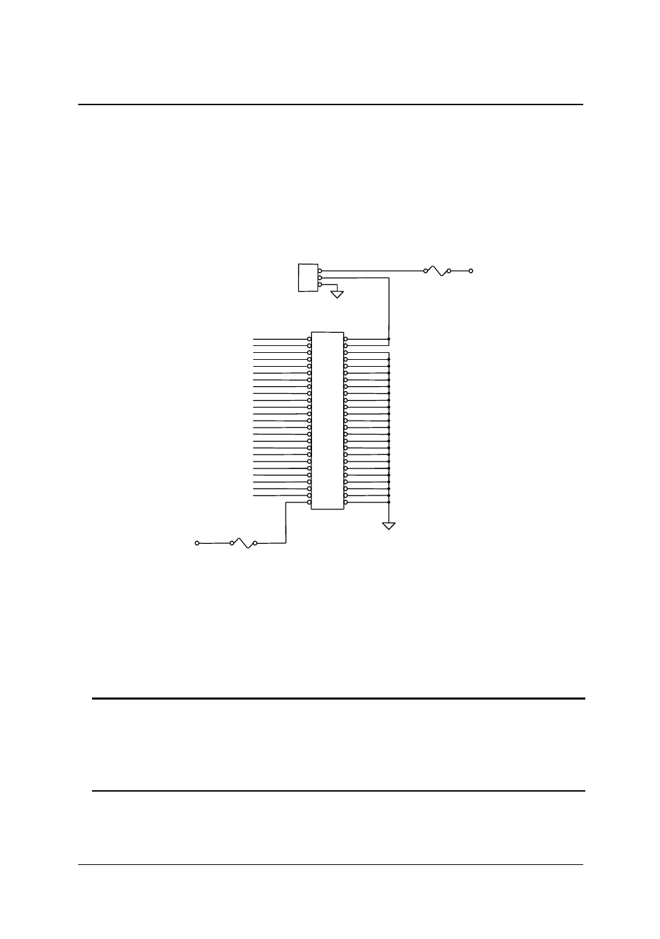
2.6.1 PCI-7224/7248/7296 Pin Assignment
The I/O ports of PCI-7224/7248/7296 emulate the mode 0 configuration of
the 8255 general purpose programmable peripheral interface. The cards
come equipped with 50-pin male IDC connectors that interface with OPTO-22.
Figure 2.4 shows the circuits and pinout of PCI-7224/7248/7296's connectors
(CN1-CN4).
1
2
3
JPn
+12V
FUSE
1
2
3
4
5
6
7
8
9
10
11
12
13
14
15
16
17
18
19
20
21
22
23
24
25
26
27
28
29
30
31
32
33
34
35
36
37
38
39
40
41
42
43
44
45
46
47
48
49
50
CNn
HEADER 25X2
PnC7
PnC6
PnC5
PnC4
PnC3
PnC2
PnC1
PnC0
PnB7
PnB6
PnB5
PnB4
PnB3
PnB2
PnB1
PnB0
PnA7
PnA6
PnA5
PnA4
PnA3
FUSE
PnA2
PnA1
PnA0
+5V
Figure 2.6.1 Pin assignments and power signals of PCI-7224/7248/7296
The DIO pin names are specified as PnXb, where
n
: means the connector reference number n=1-4.
X
: means the port name, X=A, B or C
b
: means the bit number of a port, b=0-7
For example, P1C4 means bit 4 of port C on connector CN1.
Note:
1. The pinout of the CN1-CN4 connectors are identical.
2. The power supply pins are protected by resettable fuses. Refer to section
4.4 for details on power supply.