2 vr assignment, 3 a/d adjustment – ADLINK ACL-8216 User Manual
Page 71
Calibration & Utilities • 63
6.2 VR
Assignment
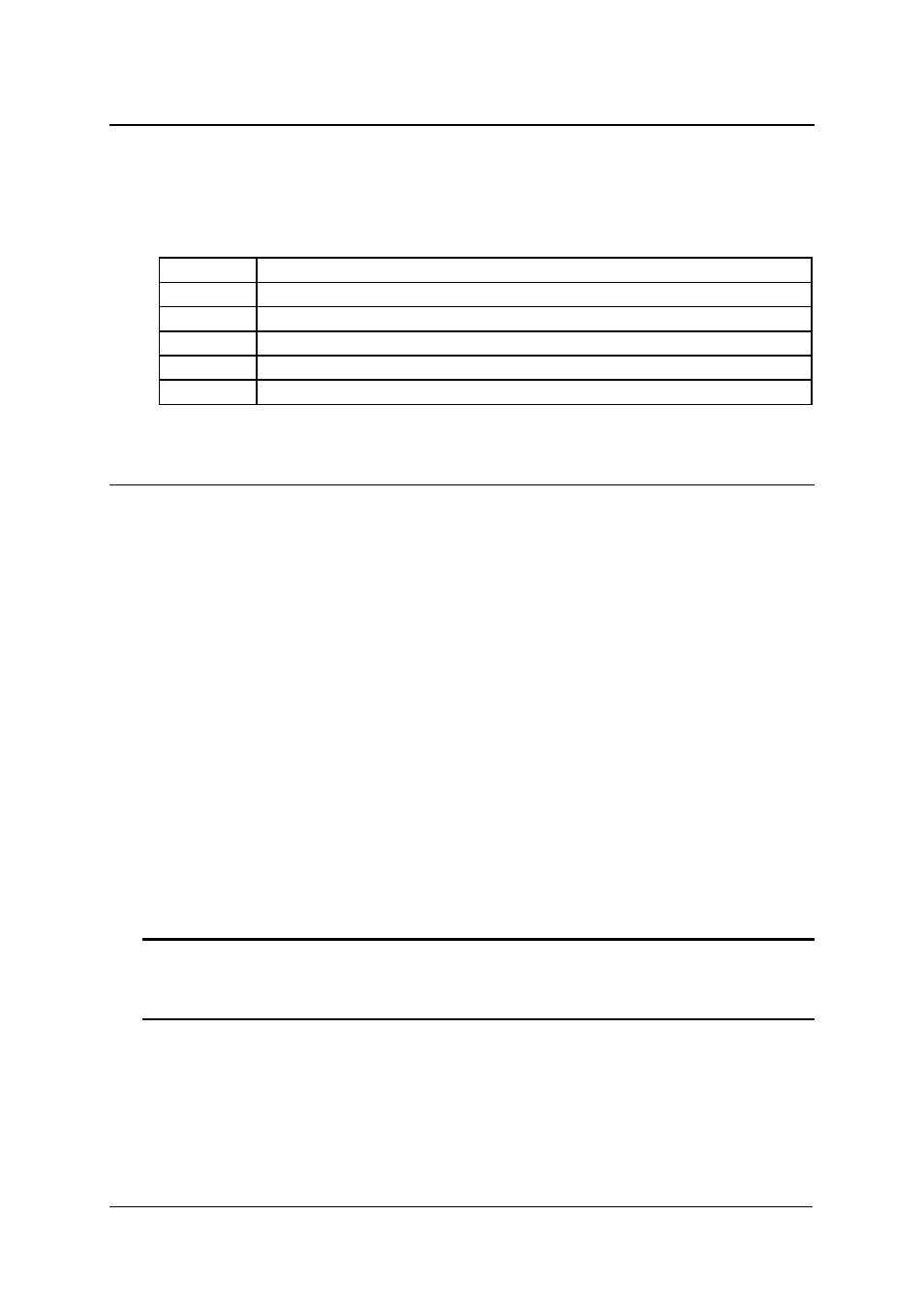
There are five variable resistors (VR) on the ACL-8216 board to allow you
making accurate adjustment on A/D and D/A channels. The function of each
VR is specified as Table 6.1.
VR1
A/D bipolar offset adjustment
VR2
A/D full scale adjustment
VR3
D/A channel 1 full scale adjustment
VR4
D/A channel 2 full scale adjustment
VR5
A/D programmable amplifier offset adjustment
VR6
D/A reference voltage adjustment
Table 6.1 Function of VRs
6.3 A/D
Adjustment
1. Set the analog input range as: +/- 10V, i.e. the gain = 1.
2. Short the A/D channel 0 ( pin 1 of CN3) to ground(GND), and connect
the TP1(+) and TP2(-) with your DVM. Trim the variable resister VR5
to obtain a value as close as possible to 0V. ( You have to keep
reading for A/D channel 0).
3. Applied a +10V input signal to A/D channel 1, and short the A/D CH0
to Analog ground( A.GND).
4. Trim VR1 until the reading of CH0 between 0000 ~ 0001(hex).
5. Trim VR2 until the reading of CH1 between 7FFE ~ 7FFF(hex).
6. Repeat step 4 and step 5, adjust until the reading values meet
requirements.
Note: When the user trims the VR1 and VR2, it will have side effect on the
D/A converted data, so repeat the step 4 and step 5 are very
important issue for A/D calibration.