Vout vref dan = − × 4096, 2 d/a conversion – ADLINK ACL-8216 User Manual
Page 44
36 • Operation Theorem
4.2 D/A
Conversion
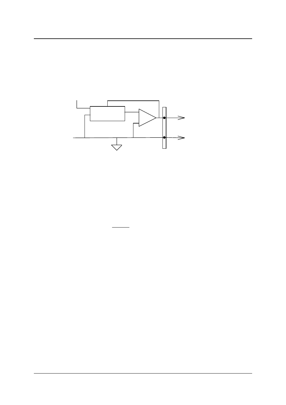
The ACL-8216 has two unipolar analog output channels. To make the D/A
output connections from the appropriate D/A output, please refer the
following figure:
To D/A Output
D/A Converter
-
+
Ref In
-5 or -10
INT or Ext
Analog GND
Pin-30 ( AO0)
Pin-32 ( AO1)
Pin-14 ( A.GND)
The operation of D/A conversion is more simple than A/D operation. You only
need to write digital values into the D/A data registers and the corresponding
voltage will be output from the AO1 or AO2. Refer to section 4.9 for
information about the D/A data registers. The mathematical relationship
between the digital number DAn and the output voltage is formulated as
following:
Vout
Vref
DAn
= −
×
4096
where the Vref is the reference voltage, the Vout is the output voltage, and
the DAn is the digital value in D/A data registers.
Before performing the D/A conversion, users should care about the D/A
reference voltage which set by the JP1,JP2 and JP3. Please refer section
2.11 for jumper setting. The reference voltage will effect the output voltage. If
the reference voltage is -5V, the D/A output scaling will be 0~5V. If the
reference voltage is -10V, the D/A output scaling will be 0~10V.
Note that the D/A registers are "double buffered", so that the D/A analog
output signals will not be updated until the high byte is written. When write
12 bits data to D/A registers of the ACL-8216, the low byte must be written
before the high byte. This procedure can insure a single step transition when
the D/A conversion.