3 a/d channel multiplexer register – ADLINK ACL-8216 User Manual
Page 33
Registers Format • 25
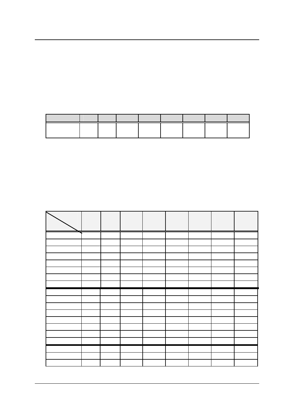
3.3 A/D Channel Multiplexer Register
This register is used to control the A/D channels to be converted. It's a write
only register. When the channel number is written to the register, the
multiplexer switches to the new channel and await for conversion.
Address : BASE + 10
Attribute: write only
Data Format:
Bit
7
6
5
4
3
2
1
0
BASE+1
0
X X CS1 CS0 CL3 CL2 CL1 CL0
CLn: multiplexer channel number.
CL2 is MSB, and CL0 is LSB.
CS0 and CS1 are used to determine which MPC508A chip is selected. The
MPC508A is used to multiplex channel from channel, when CS0 is set as 1,
the analog input channels from 0 to 7 is selectable, and CS1 is set, the ch 8
to ch 15 can be selectable. When both CS0 and CS1 are set as 1, it means
the analog input is differential mode. The possible analog input channel
selections are listed as the table below.
Bit
Channel
7
X
6
X
5
CS1
4
CS0
3
CL3
2
CL2
1
CL1
0
CL0
S.E.
CH0
X
X
0 1 0 0 0 0
S.E.
CH1
X
X
0 1 0 0 0 1
S.E.
CH2
X
X
0 1 0 0 1 0
S.E.
CH3
X
X
0 1 0 0 1 1
S.E.
CH4
X
X
0 1 0 1 0 0
S.E.
CH5
X
X
0 1 0 1 0 1
S.E.
CH6
X
X
0 1 0 1 1 0
S.E.
CH7
X
X
0 1 0 1 1 1
S.E.
CH8
X
X
1 0 1 0 0 0
S.E.
CH9
X
X
1 0 1 0 0 1
S.E.
CH10
X
X
1 0 1 0 1 0
S.E.
CH11
X
X
1 0 1 0 1 1
S.E.
CH12
X
X
1 0 1 1 0 0
S.E.
CH13
X
X
1 0 1 1 0 1
S.E.
CH14
X
X
1 0 1 1 1 0
S.E.
CH15
X
X
1 0 1 1 1 1
D.I.
CH0
X
X
1 1 0 0 0 0
D.I.
CH1
X
X
1 1 0 0 0 1
D.I.
CH2
X
X
1 1 0 0 1 0