2 a/d data registers & status control register – ADLINK ACL-8216 User Manual
Page 31
Registers Format • 23
3.2 A/D Data Registers & Status Control Register
The ACL-8216 provides 16 single-ended or 8 differential A/D input channels,
the digital data will store in the A/D data registers. The 16 bits A/D data is put
into two 8 bits registers. The low byte data (8 LSBs) are put in address
BASE+4 and the high byte data is put in address BASE+5. A Status Control
Register( Base+8) is used to check if the D/A conversion is ready. An DRDY
bit is used to indicate the status of A/D conversion. DRDY goes to low level
means A/D conversion is completed.
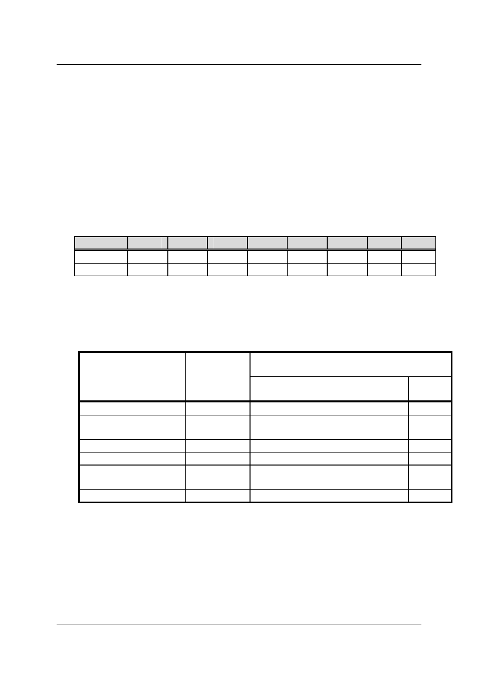
Address : BASE + 4 and BASE + 5
Attribute: read only
Data Format:
Bit
7
6
5
4
3
2
1
0
BASE+4
AD7 AD6 AD5 AD4 AD3 AD2 AD1 AD0
BASE+5 AD15 AD14 AD13 AD12 AD11 AD10 AD9 AD8
AD15 .. AD0: Analog to digital data. AD15 is the Most Significant Bit (MSB).
AD0 is the Least Significant Bit(LSB).
The A/D converted data is in Binary Two‘s Complement data output format.
Refer to Table 3.3 for ideal output code.
Description
Analog Input
Digital Output
Binary Two‘s Complement
Binary
Code
Hex
Code
Full Scale Range
±10V
Least Signification Bit
( LSB)
305
µV
+Full Scale
9.999695V
0111 1111 1111 1111
7FFF
MidScale
0V
0000 0000 0000 0000
0000
One LSB below
MidScale
-305
µV
1111 1111 1111 1111
FFFF
-Full Scale
-10V
1000 0000 0000 0000
8000
Table 3.2 Ideal Input Voltage and Output Code