Cpu base clock select (jp1) -4, Switch settings (sw1) -4, External led header (j1) -4 – Acrosser AR-B1320 User Manual
Page 23: 2 cpu base clock select (jp1), 3 switch settings (sw1), 4 external led header (j1)

A
A
R
R
-
-
B
B
1
1
3
3
2
2
0
0
U
U
s
s
e
e
r
r
’
’
s
s
G
G
u
u
i
i
d
d
e
e
3-4
3.2
CPU BASE CLOCK SELECT (JP1)
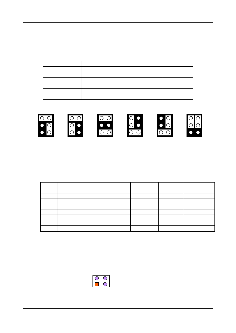
This board provides six types of CPU input clocks; they are 33.3MHz, 50MHz, 60MHz, 66.7MHz,
75MHz, and 80MHz. The CPU input clock is twice that of the operating clock. JP1 is a 6-pin
jumper located between CN3 and CN4.
CPU Input Clock
CPU Operating Clock
JP1 Setting
Remark
33.3MHz
16.7MHz
Short 1-2 & 4-6
50MHz
25MHz
Short 1-2 & 3-5
60MHz
30MHz
Short 1-2 & 5-6
66.7MHz
33.3MHz
Short 1-3 & 5-6
Factory Preset
75MHz
37.5MHz
Short 2-4 & 5-6
80MHz
40MHz
Short 1-3 & 2-4
Table 3-2 CPU Clock Settings
Figure 3-2 JP1: CPU Clock Select
3.3
SWITCH SETTINGS (SW1)
SW1 is a 6-SPST DIP switch. It provides multi-purpose selection in one switch. The following
table gives the details:
SW1
Function
When “OFF”
When “ON”
Factory Preset
Switch 1
Selects the base I/O address of SSD
210H-211H
290H-291H
Off
Switch 2
Selects the memory segment of SSD
C800H(8KB)
D800H(8KB)
Off
Switch 2 Selects the memory segment of DiskOnChip
(If Switch 3 is set as “ON”)
CA00H(8KB) DA00H(8KB)
Off
Switch 3
DiskOnChip select
Disabled
Enabled
Off
Switch 4
Reserved
---
---
Off
Switch 5
COM-A port mode select
RS-232C
RS-485
Off
Switch 6
COM-B port mode select
RS-232C
RS-485
Off
Table 3-3 SW1 Settings
3.4
EXTERNAL LED HEADER (J1)
The J1 is a 4-pin right angle header. It allows you to connect an external power LED and an
external hard disk LED.
Figure 3-3 J1: External LED Header
1
3
5
6
4
2
JP1
16.7MHz
1
3
5
6
4
2
JP1
25MHz
1
3
5
6
4
2
JP1
30MHz
1
3
5
6
4
2
JP1
33.3MHz
1
3
5
6
4
2
JP1
37.5MHz
1
3
5
6
4
2
JP1
40MHz
2
1
3
4
J1
Front View
1: Power LED+
3: Power LED-
2: Hard Disk LED+
4: Hard Disk LED-
