Ordering information, Package diagram – Cypress Quad HOTLink II CYV15G0404RB User Manual
Page 26

CYV15G0404RB
Document #: 38-02102 Rev. *C
Page 26 of 27
© Cypress Semiconductor Corporation, 2007. The information contained herein is subject to change without notice. Cypress Semiconductor Corporation assumes no responsibility for the use
of any circuitry other than circuitry embodied in a Cypress product. Nor does it convey or imply any license under patent or other rights. Cypress products are not warranted nor intended to be
used for medical, life support, life saving, critical control or safety applications, unless pursuant to an express written agreement with Cypress. Furthermore, Cypress does not authorize its
products for use as critical components in life-support systems where a malfunction or failure may reasonably be expected to result in significant injury to the user. The inclusion of Cypress
products in life-support systems application implies that the manufacturer assumes all risk of such use and in doing so indemnifies Cypress against all charges.
HOTLink is a registered trademark and HOTLink II is a trademark of Cypress Semiconductor. All product and company names
mentioned in this document may be the trademarks of their respective holders.
T03
VCC
POWER
V15
VCC
POWER
Y15
VCC
POWER
T04
VCC
POWER
V16
VCC
POWER
Y16
VCC
POWER
T17
VCC
POWER
V17
RXDA[9]
LVTTL OUT
Y17
REPDOD
LVTTL OUT
T18
VCC
POWER
V18
RXDA[5]
LVTTL OUT
Y18
TRGCLKA–
PECL IN
T19
VCC
POWER
V19
RXDA[2]
LVTTL OUT
Y19
RXDA[8]
LVTTL OUT
T20
VCC
POWER
V20
RXDA[1]
LVTTL OUT
Y20
RXDA[7]
LVTTL OUT
U01
VCC
POWER
W01
VCC
POWER
U02
VCC
POWER
W02
VCC
POWER
Table 6. Package Coordinate Signal Allocation (continued)
Ball
ID
Signal Name
Signal Type
Ball
ID
Signal Name
Signal Type
Ball
ID
Signal Name
Signal Type
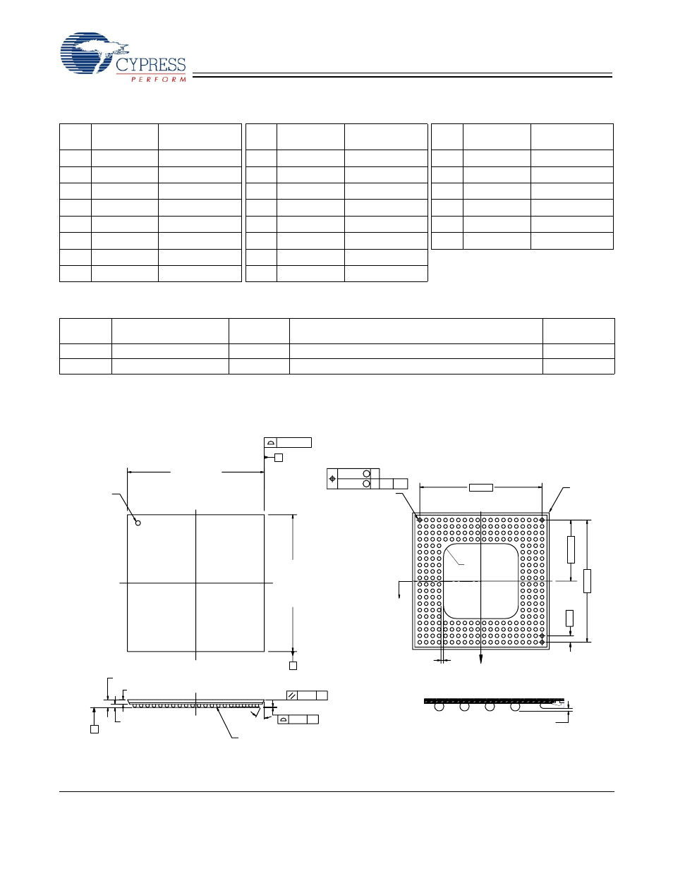
Ordering Information
Speed
Ordering Code
Package
Name
Package Type
Operating
Range
Standard
CYV15G0404RB-BGC
BL256
256-Ball Thermally Enhanced Ball Grid Array
Commercial
Standard
CYV15G0404RB-BGXC
BL256
Pb-Free 256-Ball Thermally Enhanced Ball Grid Array
Commercial
Package Diagram
Figure 3. 256-Lead L2 Ball Grid Array (27 x 27 x 1.57 mm) BL256
A
B
0.15
C
0.15
C
0.97 REF.
0.60±0.10
1.57±0.175
C
0.20 MIN
SEATING PLANE
SIDE VIEW
SECTION A-A
TOP VIEW
20
19
18
17
16
15
14
13
12
11
10
9
8
7
6
5
4
3
2
1
A
B
C
D
E
F
G
H
J
K
L
M
N
P
R
T
U
V
W
Y
A
Ø0.15 M C
Ø0.30 M C
Ø0.75±0.15(256X)
B
A
1.27
BOTTOM VIEW (BALL SIDE)
A
0.20(4X)
TOP OF MOLD COMPOUND
TO TOP OF BALLS
26°
TYP.
A1 CORNER I.D.
0.50 MIN.
27.00±0.13
27.00±0.13
24.13
24.13
A1 CORNER I.D.
R 2.5 Max (4X)
12.065
51-85123-*E
