4 memory configuration register - 12, 5 flash bank select register - 12, Memory configuration register - 12 – Kontron VMP2 User Manual
Page 64: 10 flash bank select register - 12, Vmp2 configuration

VMP2
Configuration
ID 24855, Rev. 02
Page 4 - 12
© 2002 PEP Modular Computers GmbH
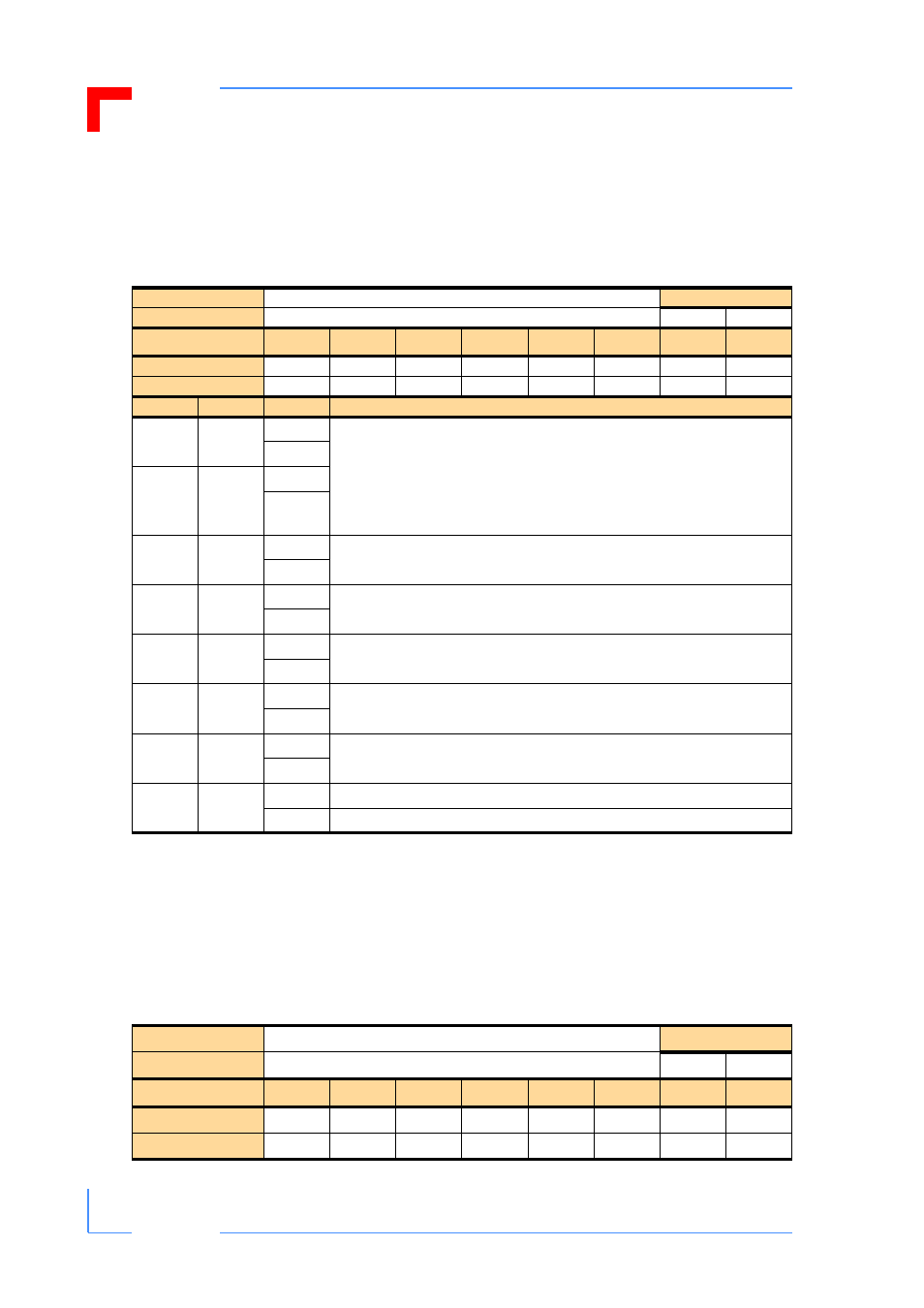
4.3.4.4 Memory Configuration Register
The Memory Configuration register provides basic information concerning the amount of
installed main memory, whether or not ECC is enabled, and the location from which the
operating system is to access the bootstrap loader.
4.3.4.5 Flash Bank Select Register
The Flash bank select register is used to select the appropriate Flash bank. As 8-bit
wide Flash memory may only be accessed through a 512 kB window; this is the only
way to address a larger size Flash memory. Using bits FB0..FB3, 16 Flash banks can be
selected (16x512 kB = 8 MB). The default value on startup of the VMP2 is 0x00.
Table 4-9: Memory Configuration Register
REGISTER NAME
MEMORY CONFIGURATION
ACCESS
ADDRESS
0xFFE0 0014
R
BIT POSITION
MSB
7
6
5
4
3
2
1
0
LSB
CONTENT
BJ
res.
res.
ECC
res.
res.
SZ1
SZ0
DEFAULT
n/a
n/a
n/a
n/a
n/a
n/a
n/a
n/a
BIT
NAME
VAL
DESCRIPTION
0
SZ0
0
Settings:
SZ1
SZ0
0
0
32 MB (64 Mbit chips, 1 bank equipped)
0
1
64 MB (64 Mbit chips, 2 banks equipped)
1
0
256 MB (256 Mbit chips, 2 bank equipped)
1
1
128 MB (128 Mbit chips, 2 bank equipped)
1
1
SZ1
0
1
2
res.
0
Reserved
1
3
res.
0
Reserved
1
4
Res.
0
Reserved
1
5
Res.
0
Reserved
1
6
Res.
0
Reserved
1
7
BJ
0
Boot Jumper J1 closed (VMP2 fetches boot code from onboard Flash)
1
Boot Jumper J1 open (VMP2 fetches boot code from socket)
Table 4-10: Flash Bank Select Register
REGISTER NAME
FLASH BANK SELECT
ACCESS
ADDRESS
0xFFE0 0016
R
W
BIT POSITION
MS
B
7
6
5
4
3
2
1
0
LS
B
CONTENT
res.
res.
res.
res.
FB3
FB2
FB1
FB0
DEFAULT
n/a
n/a
n/a
n/a
0
0
0
0
