2 pci interface, 3 rear i/o interface, Pci interface - 10 – Kontron CP346 User Manual
Page 38: Rear i/o interface - 10, Pinouts of rear i/o connector j2 - 10, Functional description cp346

Functional Description
CP346
Page 2 - 10
© 2005 Kontron Modular Computers GmbH
ID 27253, Rev. 03
P R E L I M I N A R Y
2.4.2
PCI Interface
All variants of the CP346 are equipped with the standard PCI interface connector J1. For its
pinouts please refer to the Kontron Modular Computers CompactPCI System Manual or to the
CompactPCI Specification.
2.4.3
Rear I/O Interface
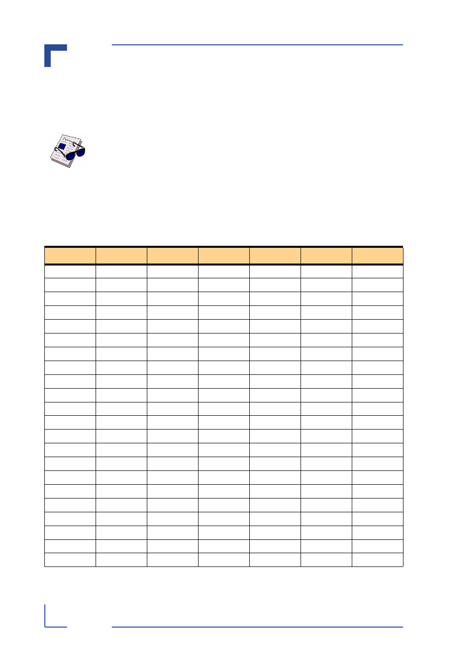
The rear I/O capable non-isolated board variant is provided with a PCI rear I/O interface con-
nector J2. All signals from the TTL serial I/O interface are routed to this connector.
N/C = not connected.
Note...
The CP346 requires 5V PCI V(I/O) signalling. It will not function properly with
3.3V V(I/O).
Table 2-3: Pinouts of Rear I/O Connector J2
Pin
Row “A”
Row “B”
Row “C”
Row “D”
Row “E”
Row “F”
1
reserved
GND
reserved
reserved
N/C
GND
2
reserved
+5V
reserved
reserved
N/C
GND
3
N/C
GND
N/C
N/C
reserved
GND
4
N/C
+5V
N/C
GND
reserved
GND
5
N/C
GND
N/C
N/C
N/C
GND
6
N/C
+5V
RI2
GND
N/C
GND
7
RI3
GND
N/C
RI1
RI0
GND
8
DCD3
+5V
DCD2
GND
DCD0
GND
9
DSR3
GND
N/C
DCD1
DSR0
GND
10
CTS3
+5V
DSR2
GND
CTS0
GND
11
RxD3
GND
N/C
DSR1
RxD0
GND
12
DTR3
+5V
CTS2
GND
DTR0
GND
13
RTS3
GND
N/C
CTS1
RTS0
GND
14
TxD3
+5V
RxD2
GND
TxD0
GND
15
N/C
GND
DTR2
RxD1
N/C
GND
16
+5V
+5V
RTS2
GND
+5V
GND
17
N/C
GND
TXD2
DTR1
N/C
GND
18
+5V
N/C
+5V
GND
+5V
GND
19
GND
GND
N/C
RTS1
N/C
GND
20
N/C
GND
N/C
GND
N/C
GND
21
N/C
GND
N/C
TxD1
N/C
GND
22
N/C
N/C
N/C
N/C
N/C
GND
