Ac operating conditions, Dc electrical specifications, Ac operating condi – Cypress Rambus XDR CY24271 User Manual
Page 8: Tions
CY24272
Document Number: 001-42414 Rev. **
Page 8 of 13
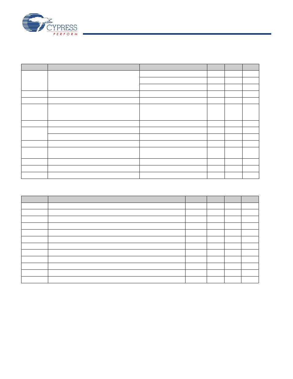
AC Operating Conditions
The AC operating conditions follow.
Parameter
Description
Condition
Min
Max
Unit
t
CYCLE,IN
REFCLK, REFCLKB input cycle time
REFSEL = 0, /BYPASS = High
9
11
ns
REFSEL = 1, /BYPASS = High
7
8
ns
/BYPASS = Low
4
–
ns
t
JIT,IN(cc)
Input Cycle to Cycle Jitter
–
185
ps
t
DCIN
Input Duty Cycle
Over 10,000 cycles
40%
60%
t
CYCLE
t
RIN
/ t
FIN
Rise and Fall Times
Measured at 20%–80% of input
voltage for REFCLK and
REFCLKB inputs
175
700
ps
Δt
RIN
/ t
FIN
Rise and Fall Times Difference
–
150
ps
p
MIN
Modulation Index for triangular modulation
–
0.6
%
Modulation Index for non-triangular modulation
–
0.5
%
f
MIN
Input Frequency Modulation
30
33
kHz
t
SR,IN
Input Slew Rate (measured at 20%–80% of
input voltage) for REFCLK
1
4
V/ns
C
IN,REF
Capacitance at REFCLK inputs
–
7
pF
C
IN,CMOS
Capacitance at CMOS inputs
–
10
pF
f
SCL
SMBus clock frequency input in SCL pin
DC
100
kHz
DC Electrical Specifications
Parameter
Description
Min
Typ
Max
Unit
V
OX
Differential output crossing point voltage
–
1.08
–
V
V
COS
Output voltage swing (peak-to-peak single-ended)
–
400
–
mV
V
OL,ABS
Absolute output low voltage at CLK[3:0], CLK[3:0]B
0.85
–
–
V
V
ISET
Reference voltage for swing controlled current, I
REF
0.98
1.0
1.02
V
I
DD
[7]
Power Supply Current at 2.625V, f
ref
= 100 MHz, and f
out
= 300 MHz
–
–
85
mA
I
DD
[7]
Power Supply Current at 2.625V, f
ref
= 133 MHz, and f
out
= 667 MHz
–
–
125
mA
I
OL/
I
REF
Ratio of output low current to reference current
6.8
7.0
7.2
I
OL,ABS
Minimum current at V
OL,ABS
25
–
–
mA
V
OL,SDA
SDA output low voltage at test condition of SDA output low current = 4 mA
–
–
0.4
V
I
OL,SDA
SDA output low voltage at test condition of SDA voltage = 0.8V
6
–
–
mA
I
OZ
Current during High Z per pin at CLK[3:0], CLK[3:0]B
–
–
10
μA
Z
OUT
Output dynamic impedance when clock output signal is at V
OL
= 0.9V
1000
–
–
Ω
Notes
9. Jitter measured at crossing points and is the absolute value of the worst case deviation.
10. Measured at crossing points.
11. If input modulation is used; input modulation is allowed but not required.
12. The amount of allowed spreading for any non-triangular modulation is determined by the induced downstream tracking skew that cannot exceed the skew generated
by the specified 0.6% triangular modulation. Typically, the amount of allowed non-triangular modulation is about 0.5%.
13. V
OX
is measured on external divider network.
14. V
COS
= (clock output high voltage – clock output low voltage), measured on the external divider network.
15. V
OL_ABS
is measured at the clock output pins of the package.
16. I
REF
is equal to V
ISET
/R
RC
.
17. Minimum I
OL,ABS
is measured at the clock output pin with R
RC
= 266 ohms or less.
18. Z
OUT
is defined at the output pins as (0.94V – 0.90V)/(I
0.94
– I
0.90
) under conditions specified for I
OL, ABS
.