Block diagram, I/o connections, R20ce 10-bit encoder, block diagram – AJA R20CE User Manual
Page 4
4
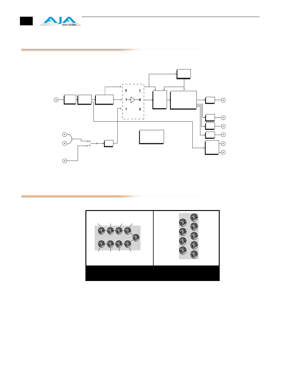
Block Diagram
R20CE 10-bit Encoder, Block Diagram
I/O Connections
FR1 and FR2 BNC Connector Assignments, R20CE Card Module
When the R20CE module is installed in an AJA FR1 or FR2 frame, a corresponding
group of 9 BNCs on the rear panel then provide I/O for the module. The
illustration above shows the connector assignments for both the FR1 and FR2
when used with the R20CE.
Note:
See the topic “
External Reference Information
” later in this manual for
information on use of the
Ref Loop
BNCs versus the FR1/FR2 frame reference BNC
when connecting an external reference video signal.
1
2
Cable
EQ
Serial
Video
In
Serial/
Parallel
REF
LOOP
FRAME
REF
Filter
Filter
Filter
Filter
Filter
Cable
Driver
Serial
Out
PIC
Microcontroller
Clock
Filter
FIFO
Encoder
27 MHz
27 MHz
27 MHz
Bypass
ReClock
COMPOSITE
COMP/_/G/Y
COMP/Y/B/B-Y
COMP/C/R/R-Y
Frame
Mezzanine
(optional)
J1
J3
J5
J7
J9
J2
J4
J6
J8
J1
J2
J3
J4
J5
J6
J7
J8
J9
FR1 Frame Layout
R20CE Rear Panel
FR2 Frame Layout
R20CE Rear Panel
SDI In
SDI Out 2
Ref Loop
CMPST Out
CMPST/
Y/B/Pb
SDI Out 1
Ref Loop
CMPST -/G/Y Out
CMPST/
C/R/Pr
SDI In
SDI
Out 2
SDI
Out 1
Ref
Loop
Ref
Loop
CMPST
Out
CMPST
Y/B/Pb
Out
CMPST/
G/Y Out
CMPST
C/R/Pr
Out