3 boost inductor design, 4 pcb layout changes, 5 auxiliary supply design – Cirrus Logic AN349 User Manual
Page 10: An349, Table 1. boost inductor comparison, Table 2. v, Generation, Cs1601

AN349
10
AN349REV1
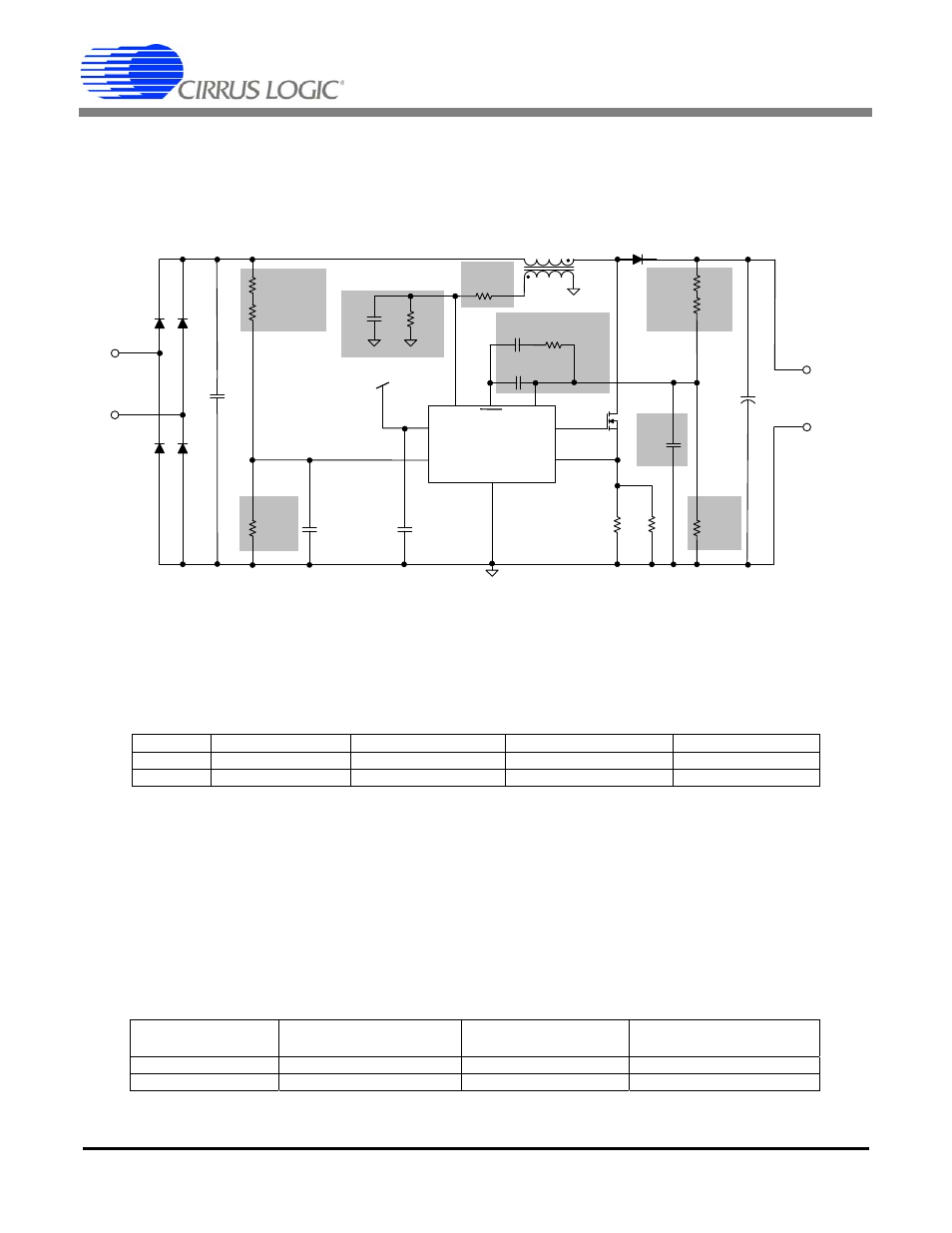
Make changes to the schematic as shown. Note that capacitor C6 can be between pin 1 and GND or pin 1 and VDD, based on
routing considerations. Also, capacitor C2 can be between pin 3 and GND or pin 3 and VDD. Refer to application note AN346 -
CS1501 & CS1601 PCB Layout Guidelines for further information.
It is recommended to place a 33 pF capacitor (C8) between pin 5 and GND. It is important that the capacitor be at close to the
pins as possible. Also, the ground side of the capacitor should be placed away from the gate drive ground return path.
Figure 13. PFC Schematic Of Benchmark Ballast Using CS1601
6.3 Boost Inductor Design
The difference in the boost inductor can be understood from Figure 8 and Figure 9. For the fluorescent ballast under study, the
inductor difference is shown in table below.
Table 1. Boost Inductor Comparison
6.4 PCB Layout Changes
The signal ground of the ballast should be re-routed to reference the negative of the current-sense resistor. Depending on the
distance, another place where the ground can be referenced is the negative of the electrolytic bulk capacitor. Resistor R3 is ref-
erenced to be close to the 100nF capacitor. Refer to application note AN346 - CS1501 & CS1601 PCB Layout Guidelines for
detailed information on best layout practices when designing systems based upon the CS1601.
6.5 Auxiliary Supply Design
There are many ways to design the auxiliary supply. However, the table below shows some differences between L6562 and
CS1601 with respect to aux supply design.
Table 2. V
CC
Generation
CHANGE
CHANGE
ADD
DELETE
DELETE
DELETE
CHANGE
ADD
R1
1. 72M
R2
1.72M
R5
68k
R7
0. 82
0.6W
R10
1.72M
R11
1.72M
8
1
D1
C1
. 47 uF
400V
C7
100uF
Regulated
DC Output
Q1
AC
Mains
BR1
BR1
BR1
BR 1
CS1601
GD
ZCD
IFB
GND
CS
IAC
VDD
L
B
6
3
5
7
4
V
DD
R9
9.53k
C4
2.2 uF
R6
12k
R3
22k
C2
100pF
2
C5
680 nF
R4
1. 75k
C3
4. 7uF
R8
0. 82
0.6W
C6
100pF
25V
STBY
C8
33 pF
IC
Inductance (uH)
Peak Current (A)
Turns Ratio (Np:Ns)
Frequency (KHz)
L6562 700
4.5
10
45
CS1601 380
4.5
10
70
IC
Min Vcc @
Turn ON (V)
Max Vcc @
Turn OFF (V)
Nominal Vcc (V)
L6562 13
10
11
-22
CS1601 10.8
8.5
9
-17
