7 power, 8 grounding and power supply decoupling, 7 power 1.8 grounding and power supply decoupling – Cirrus Logic CDB8421 User Manual
Page 6: Table 5. switch s4, board setup, Cdb8421
CDB8421
6
DS641DB3
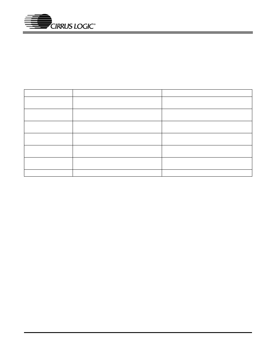
Switch S4 allows any of the PCM clocks/data to be turned off, selection between the OPTI-
CAL and COAXIAL S/PDIF inputs, bypassing the CS8421 sample rate converter, and turning
off the CS8421 MCLK_OUT signal. To input and output S/PDIF to and from the CS8421, the
switches labeled 8416_PCM, 8421_INPUT_PCM, 8421_OUTPUT_PCM, and 8406_PCM
should all be set in the CLOSED position. The functions for switches S4[6:0] are detailed in
Table 5.
NOTE:The reset button must be pressed before a new mode of operation takes affect.
Some speed modes and switch combinations are not compatible with the CS8416, CS8421,
or the CS8406. LED’s D4, D5, and D7 indicate that a switch setting is not compatible with the
corresponding part.
1.7
Power
Power must be supplied to the evaluation board through the +5.0 V binding post (J1). On-
board regulators supply +3.3 V and +2.5 V to the rest of the board. Jumper J3 sets the VL
supply of the CS8416, CS8421, and CS8406 to either +3.3 V or +5.0 V. All voltage inputs
must be referenced to the single black banana-type ground connector (J2).
WARNING:Please refer to the CS8421 data sheet for allowable voltage levels.
1.8
Grounding and Power Supply Decoupling
The CS8421 requires careful attention to power supply and grounding arrangements to opti-
mize performance. Figure 1 provides an overview of the connections to the CS8421,
Figure 10 shows the component placement, Figure 11 shows the top layout, and Figure 12
shows the bottom layout. The decoupling capacitors are located as close to the CS8421 as
possible. Extensive use of ground plane fill in the evaluation board yields large reductions in
radiated noise.
Switch Name
OPEN
CLOSED
8416_PCM
Inhibits Clock I/O and Data Output from
CS8416 to Header J8
Allows Clock I/O and Data Output from
CS8416 to Header J8
8421_INPUT_PCM
Inhibits Clock I/O and Data Input from
Header J8 to CS8421
Allows Clock I/O and Data Input from
Header J8 to CS8421
8421_OUPUT_PCM
Inhibits Clock I/O and Data Output from
CS8421 to Header J11
Allows Clock I/O and Data Output from
CS8421 to Header J11
8406_PCM
Inhibits Clock I/O and Data Output from
Header J11 to CS8406
Allows Clock I/O and Data Output from
Header J11 to CS8406
8416_RXSEL
Selects Coaxial Connector (J5) for S/PDIF
Input
Selects Optical Receiver (J12) for S/PDIF
Input
8421_BYPASS
Selects CS8421 SRC Bypass Mode (no
sample rate conversion)
Selects CS8421 SRC Active Mode
8421_MCLK_OUT
CS8421 MCLK_OUT Pin Held Low
CS8421 MCLK_OUT Pin Active
Table 5. Switch S4, Board Setup