Controlling digital signal noise, Optimizing the input span, Figure 4 – Cirrus Logic AN299 User Manual
Page 5: An299
AN299REV1
5
AN299
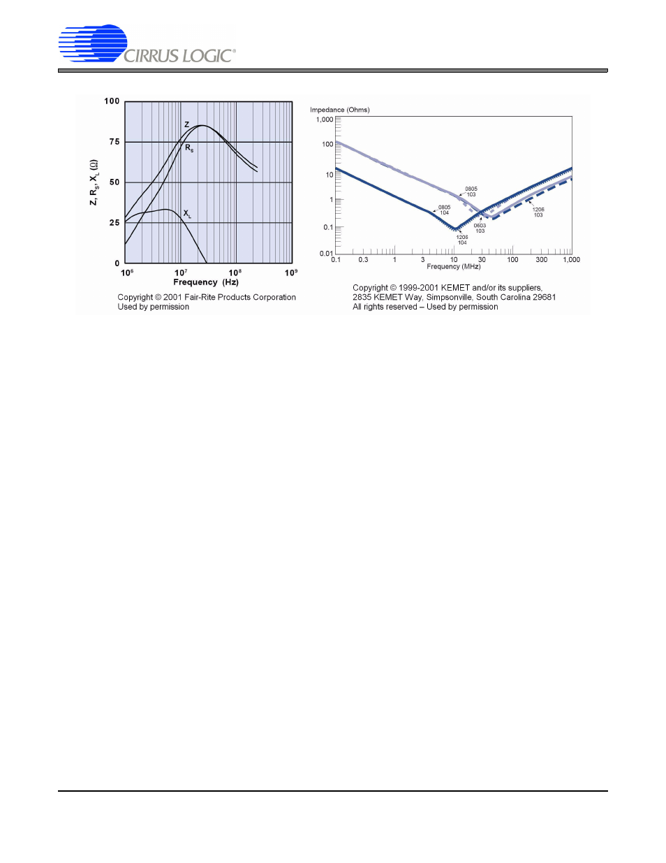
Figure 4. Ferrite Bead and X7R Ceramic Capacitor Impedance vs. Frequency
4. CONTROLLING DIGITAL SIGNAL NOISE
The ADC is a mixed-signal device and has digital as well as analog pins. Therefore, in most applications, there are
relatively high-energy digital signals in close proximity to very low-level analog signals - especially near the ADC
itself. Thus, great caution should be used to assure that the digital signals do not corrupt the low-level analog signals.
Two methods that have already been mentioned should be used –
avoiding high-speed signals crossing splits in
the power or ground planes and avoiding locating digital ports that leave the board near the ADC.
Whether a crystal is used with the internal crystal oscillator or an external oscillator is used, the routing of the clock
traces to the ADC should be carefully placed. Again, avoid allowing the clock signals to cross a split in the power
and ground planes and route the clock as far from AIN and VREF signals as possible.
External clock oscillators and microcontroller or microprocessor serial bus signals often have much faster edges
than are required by the ADC. These fast edges along with circuit board parasitic capacitance and inductance often
create reflections and high-energy harmonics into the hundreds of megahertz. One effective way to minimize these
reflections and harmonics is to put a damping resistor in series with the trace as close to the source pin as possible.
For example, the SCLK and SDI signals from a microprocessor or microcontroller could have 20- to 50-ohm series
resistors at the microprocessor pins and the SDO signal could likewise have a 20- to 50-ohm resistor at the ADC
SDO pin. The actual value of the resistor will depend on the board parasitics and trace lengths and could be deter-
mined by simulation software (such as HyperLynx
®
from Mentor Graphics
®
) or it could be determined empirically
after the board is built by observing the signal with a low capacitance oscilloscope probe. Using the probe, the small-
est resistor value that eliminates overshoot and undershoot and other reflection induced artifacts should be used.
Obviously too large a resistor value will result in excessive slewing of the digital signals and may compromise the
noise immunity of the digital interface. Generally the resistor value should be 50 ohms or less.
5. OPTIMIZING THE INPUT SPAN
The CS5531/32/33/34 delta-sigma converters have a built-in digital filter and calibration engine. The delta-sigma
modulator generates a single-bit bitstream of 307,200 bits per second (assuming a 4.9152 MHz crystal or oscillator
and FRS = 0) which is the input to the digital filter. From this bitstream the digital filter creates a parallel digital word
representative of the analog input voltage. The calibration engine takes this digital value (which has more resolution
than the output word), adds the offset correction from that channel's offset calibration register, and then multiplies
that result by the contents of the gain calibration register for that channel. This result is then truncated to