Decoupling (bypass) capacitors, Figure 3, An299 – Cirrus Logic AN299 User Manual
Page 3
AN299REV1
3
AN299
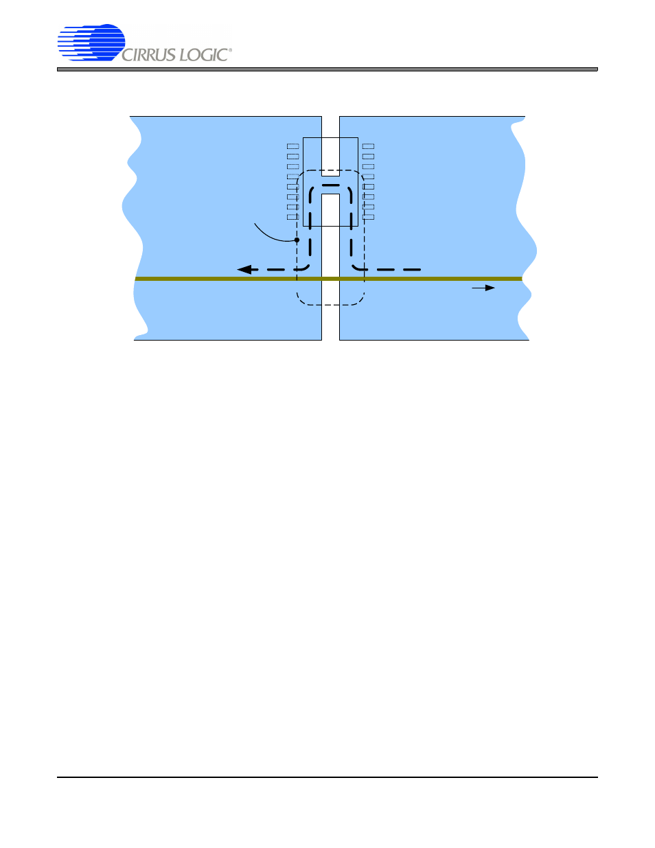
Figure 3. Antenna Loop Caused by Ground or Power Plane Splits
It is important to note that the CS5531/2/3/4 devices do not have an AGND pin. The common-mode reference for
the analog inputs is VA- (the die substrate). In single-supply configurations it is important that VA- be connected to
the DGND pin through a low-impedance ground plane. In dual-supply configurations the bypass capacitors on VA-
and VA+ should be connected to the same ground as the DGND pin through low-ESR (effective series resistance)
bypass capacitors. The reason for this is that any noise differential between these pins will result in noise from the
digital core ground (DGND pin) getting into the internal analog circuitry through the level shifters and parasitic ca-
pacitance on the die. Also, any noise differential between the VA- pin and the anti-aliasing capacitors on the analog
inputs will result in common-mode noise being directly coupled to the inputs. Although the ADC has an excellent
common-mode rejection ratio (CMRR) at DC and low frequencies, the higher the frequency of the common mode
noise, the more likely it is that it will be sampled by the ADC and aliased into the pass band. This is especially true
of noise from switch-mode power supplies.
In general, the ADC should be located such that any heavy dynamic currents flowing in the ground plane are kept
away from the converter. This may require that the converter be located on the PCB as far from the power connec-
tions as possible. Furthermore, digital IO ports that leave the PCB should not be located near the ADC. The transient
currents these ports often must provide to charge parasitic capacitance on the cabling can create significant noise
differentials in the ground plane. If these guidelines are followed it may not be necessary to use separate analog
and digital ground planes. Therefore the problem of high-speed signals crossing splits in the plane is avoided.
3. DECOUPLING (BYPASS) CAPACITORS
As noted previously, the choice and placement of capacitors for power supply decoupling is very important. The sup-
ply currents to mixed-signal devices are dynamic, not steady-state DC. If this dynamic current was supplied only by
a power source located away from the ADC, very large fluctuations in the voltages at the power pins of the device
would be seen as a result of the series impedances between the device and the power source. Therefore, capacitors
are required at the power pins of the device to act as a reservoir of charge for these dynamic currents. For this rea-
son, these capacitors must be located as close as physically possible to the power pins in order to minimize the
series impedance between the power pins and the capacitors. The bypass capacitors for VA+ and VA- should be
between these power pins instead of from each pin to ground since they provide a reservoir of charge between the
AGND
DGND
Return Current
Loop antenna effect
radiates high-frequency
energy to other traces
High-speed Digital Signal Trace On Adjacent Layer