An44rev2 3 – Cirrus Logic AN44 User Manual
Page 3

CS5508 EXAMPLE
The following example uses a CS5508 to
illustrate the process of designing a modified
serial cable. By examining the schematic for the
CDB5508 evaluation board, the digital interface
circuitry is identified. The schematic for the
CDB5508 evaluation board is provided in Figure
1 of the CDB5505/6/7/8 data sheet. The digital
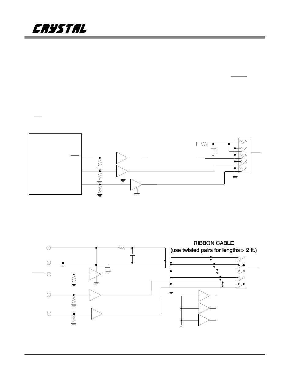
interface portion is shown in Figure 2 below.
Resistors R23, R24 and R25 are not required if
the CS is always active. Also, U3B is always
active when using the CAPTURE board, thus it
can be changed to a general purpose buffer such
as U2.
Figure 3 shows the schematic for the modified
cable derived from Figure 2. The DRDY, SCLK
and SDATA signals are buffered to create the
serial cable signals for the CAPTURE board.
Five volt power is obtained from the embedded
system and filtered by R1 and C1 before it is
provided to the CAPTURE board. C2 is a
bypass capacitor for U1.
U3B
5
6
4
U2F
8
15
14
U2E
12
11
SCLK
DRDY
SDATA
+5
C16
10 uF
R22
10
+
R25
100k
R24
100k
R23
100k
+5
+5
SCLK
SDATA
DRDY
14
15
16
U1
CS5505
CS5506
CS5507
OR
CS5508
Figure 2. CDB5508 Evaluation Board Schematic for the Digital Interface
U1D
9
10
U1E
11
12
U1F
14
15
U1C
7
6
U1B
8
4
5
U1A
2
3
SCLK
DRDY
SDATA
C1
10 uF
R1
10
+
R4
100k
R3
100k
R2
100k
+5
+5
C2
0.1 uF
1
+5 V
GND
DRDY
SCLK
SDATA
HC4050
Figure 3. Modified Serial Cable Implementation of the Digital Interface
Using The CDBCapture System with Embedded A/D Converters
AN44REV2
3
