Vrefout reference output voltage, 5v digital characteristics, Cs5460a – Cirrus Logic CS5460A User Manual
Page 7
CS5460A
DS487F5
7
VREFOUT REFERENCE OUTPUT VOLTAGE
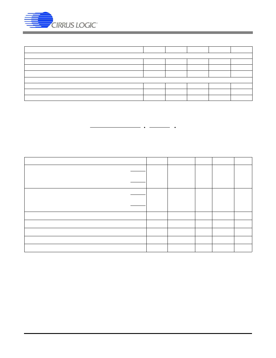
Notes: 12. The voltage at VREFOUT is measured across the temperature range. From these measurements the
following formula is used to calculate the VREFOUT Temperature Coefficient:.
5V DIGITAL CHARACTERISTICS
(T
A
= -40 °C to +85 °C; VA+ = VD+ = 5 V ±10% VA-, DGND = 0 V) (See Notes 3, 4, and 13)
13. Note that the 5 V characteristics are guaranteed by characterization. Only the more rigorous 3.3 V
digital characteristics are actually verified during production test.
14. Applies to all INPUT pins except XIN pin (leakage current < 50 µA) and MODE pin (leakage current <
25 µA).
Parameter
Symbol Min
Typ
Max
Unit
Reference Output
Output Voltage
REFOUT
+2.4
-
+2.6
V
VREFOUT Temperature Coefficient
(Note 12) T
VREFOUT
-
30
60
ppm/°C
Load Regulation
(Output Current 1 µA Source or Sink)
V
R
-
6
10
mV
Reference Input
Input Voltage Range
VREFIN
+2.4
+2.5
+2.6
V
Input Capacitance
-
4
-
pF
Input CVF Current
-
25
-
nA
Parameter
Symbol Min Typ
Max
Unit
High-Level Input Voltage
All Pins Except XIN, SCLK and RESET
XIN
SCLK and RESET
V
IH
0.6 VD+
(VD+) - 0.5
0.8
VD+
-
-
-
-
-
-
V
V
V
Low-Level Input Voltage
All Pins Except XIN, SCLK, and RESET
XIN
SCLK and RESET
V
IL
-
-
-
-
-
-
0.8
1.5
0.2
VD+
V
V
V
High-Level Output Voltage (except XOUT)
I
out
= +5 mA
V
OH
(VD+) - 1.0
-
-
V
Low-Level Output Voltage (except XOUT)
I
out
= -5 mA
V
OL
-
-
0.4
V
Input Leakage Current
I
in
-
±1
±10
µA
High Impedance State Leakage Current
I
OZ
-
-
±10
µA
Digital Output Pin Capacitance
C
out
-
5
-
pF
(VREFOUT
MAX
-
VREFOUT
MIN
)
VREFOUT
AVG
T
A
MAX
-
T
A
MIN
1
(
(
)
)
1.0 x 10
(
)
6
T
VREFOUT
=