Cirrus Logic CS5460A User Manual
Features, Description, On-chip functions: (real) energy, i v, i

1
Copyright
Cirrus Logic, Inc. 2011
(All Rights Reserved)
Cirrus Logic, Inc.
http://www.cirrus.com
CS5460A
Single Phase, Bi-directional Power/Energy IC
Features
Energy Data Linearity: ±0.1% of Reading
over 1000:1 Dynamic Range.
On-Chip Functions: (Real) Energy, I
V,
I
RMS
and V
RMS
, Energy-to-Pulse
Conversion
Smart “Auto-boot” Mode from Serial
EEPROM Enables Use without MCU.
AC or DC System Calibration
Mechanical Counter/Stepper Motor Driver
Meets Accuracy Spec for IEC 687/1036, JIS
Typical Power Consumption <12 mW
Interface Optimized for Shunt Sensor
V vs. I Phase Compensation
Ground-Referenced Signals with Single
Supply
On-chip 2.5 V Reference (MAX 60 ppm/°C
drift)
Simple Three-wire Digital Serial Interface
Watch Dog Timer
Power Supply Monitor
Power Supply Configurations
VA+ = +5 V; VA- = 0 V; VD+ = +3.3 V to +5 V
Description
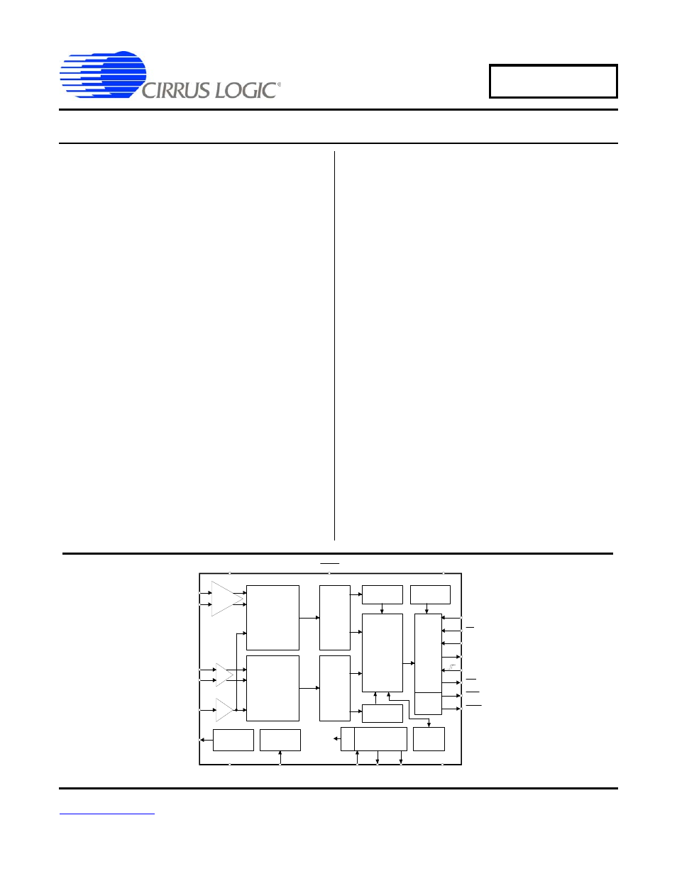
The CS5460A is a highly integrated power mea-
surement solution which combines two
Analog-to-digital Converters (ADCs), high-speed
power calculation functions, and a serial interface
on a single chip. It is designed to accurately mea-
sure and calculate: Real (True) Energy,
Instantaneous Power, I
RMS
, and V
RMS
for single
phase 2- or 3-wire power metering applications.
The CS5460A interfaces to a low-cost shunt resis-
tor or transformer to measure current, and to a
resistive divider or potential transformer to mea-
sure voltage. The CS5460A features a
bi-directional serial interface for communication
with a microcontroller and a pulse output engine for
which the average pulse frequency is proportional
to the real power. The CS5460A has on-chip func-
tionality to facilitate AC or DC system-level
calibration.
The “Auto-boot” feature allows the CS5460A to
function ‘stand-alone’ and to initialize itself on sys-
tem power-up. In Auto-boot Mode, the CS5460A
reads the calibration data and start-up instructions
from an external EEPROM. In this mode, the
CS5460A can operate without a microcontroller, in
order to lower the total bill-of-materials cost.
PGA
x10,x50
VA+
VD+
IIN+
IIN-
VIN+
VIN-
VREFIN
VREFOUT
VA-
XIN
XOUT CPUCLK
DGND
CS
SDO
SDI
SCLK
INT
EOUT
Digital
Filter
High Pass
Filter
Voltage
Reference
System
Clock
/K
Clock
Generator
Serial
Interface
Power
Calculation
Engine
(Energy
I * V
I
,V
)
RMS
RMS
Energy-to-
Pulse
Converter
Power
Monitor
PFMON
x1
x10
4
Order
Modulator
th
RESET
Digital
Filter
Calibration
SRAM
EDIR
High Pass
Filter
2
Order
Modulator
nd
Watch Dog
Timer
MODE
Control /
APR ‘11
DS487F5
Document Outline
- Features
- 1. Characteristics & Specifications
- 2. Overview
- 3. Functional Description
- 3.1 Pulse-Rate Output
- 3.2 Pulse Output for Normal Format, Stepper Motor Format and Mechanical Counter Format
- 3.3 Auto-boot Mode Using EEPROM
- 3.4 Interrupt and Watchdog Timer
- 3.5 Oscillator Characteristics
- 3.6 Analog Inputs
- 3.7 Voltage Reference
- 3.8 Calibration
- 3.9 Phase Compensation
- 3.10 Time-Base Calibration Register
- 3.11 Power Offset Register
- 3.12 Input Protection - Current Limit
- 3.13 Input Filtering
- 3.14 Protection Against High-voltage and/or High-current Surges
- 3.15 Improving RFI Immunity
- 3.16 PCB Layout
- 4. Serial Port Overview
- 5. Register Descriptions
- 6. Pin Descriptions
- 7. Package Dimensions
- 8. Ordering Information
- 9. Environmental, Manufacturing, & Handling Information
- 10. Revision History
