Pin description, Cs5373a – Cirrus Logic CS5373A User Manual
Page 36
CS5373A
36
DS703F2
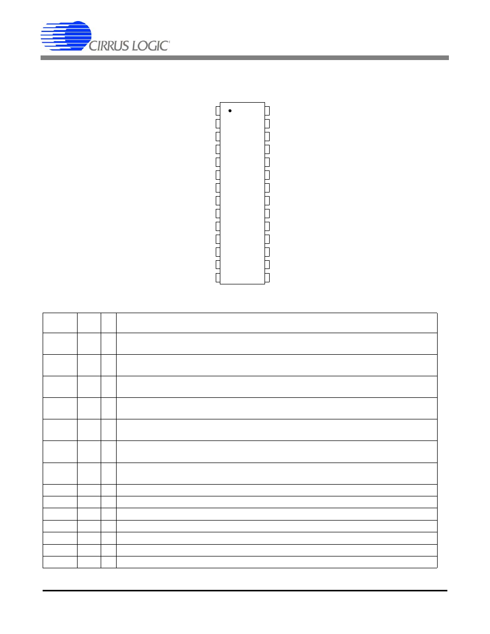
11. PIN DESCRIPTION
1
2
3
4
5
6
7
8
21
22
23
24
25
26
27
28
9
10
11
12
17
18
19
20
13
14
15
16
Positive Capacitor Output
CAP+
Negative Capacitor Output
CAP-
Positive Buffered Output
BUF+
Negative Buffered Output
BUF-
Positive High Precision Output
OUT+
Negative High Precision Output
OUT-
Positive Analog Power Supply
VA+
Negative Analog Power Supply
VA-
Negative Voltage Reference
VREF-
Positive Voltage Reference
VREF+
Positive Analog Rough Input
INR+
Positive Analog Fine Input
INF+
Negative Analog Fine Input
INF-
Negative Analog Rough Input
INR-
GND
System Ground
MODE0
Mode Select
MODE1
Mode Select
MODE2
Mode Select
ATT0
Attenuation Range Select
ATT1
Attenuation Range Select
ATT2
Attenuation Range Select
TDATA
Test Bit Stream Input
VD
Positive Digital Power Supply
GND
System Ground
MCLK
Master Clock Input
MSYNC
Master Sync Input
MDATA
Modulator Data Output
MFLAG
Modulator Over-range Indicator
Pin
Name
Pin # I/O
Pin Description
CAP+,
CAP-
1
2
O
Capacitor connection for internal anti-alias filter.
BUF+,
BUF-
3
4
O
Buffered differential analog output.
OUT+,
OUT-
5
6
O
Precision differential analog output.
VA+,
VA-
7
8
Analog power supply. Refer to the Specified Operating Conditions.
VREF-,
VREF+
9
10
I
Voltage reference input. Refer to the Specified Operating Conditions.
INR+,
INF+
11
12
I
Analog differential rough and fine + inputs. From the + half of the differential anti-alias fil-
ter.
INF-,
INR-,
13
14
I
Analog differential rough and fine - inputs. From the - half of the differential anti-alias filter.
MFLAG
15
O
Amplitude overload indicator flag.
MDATA
16
O
Oversampled
ΔΣ bit stream conversion output.
MSYNC
17
I
Master sync input. Low to high transition resets the internal clock phasing.
MCLK
18
I
Master clock input. CMOS compatible clock input.
GND
19
System ground.
VD
20
Digital power supply. Refer to the Specified Operating Conditions.
TDATA
21
I
Test Bit Stream input from digital filter TBS generator.