Analog signals, 1 inr±, inf± modulator inputs, 1 modulator input impedance – Cirrus Logic CS5373A User Manual
Page 28: 2 modulator anti-alias filter, Cs5373a, Figure 14. analog signals
CS5373A
28
DS703F2
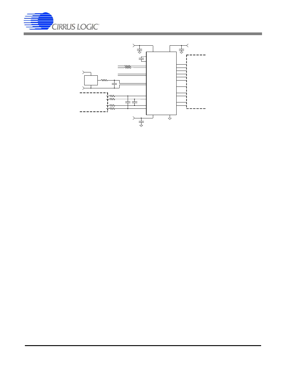
7. ANALOG SIGNALS
The CS5373A has multiple differential analog
inputs and outputs. The modulator analog in-
puts are separated into rough and fine charge
differential pairs (INR±, INF±) for maximum
sampling accuracy. Both sets of modulator in-
puts require a simple differential anti-alias RC
filter to ensure high-frequency signals do not
alias into the measurement bandwidth.
The test DAC has a precision differential out-
put (OUT±) that provides the best analog per-
formance, but with only minimal drive
capability. A buffered output (BUF±) can drive
an external load, but with reduced analog per-
formance. Finally, the test DAC internal anti-
alias filter requires a dedicated capacitor con-
nection (CAP±) to eliminate undesired high-
frequency signals.
7.1 INR±, INF± Modulator Inputs
The modulator analog inputs are separated
into differential rough and fine signals (INR±,
INF±). The positive half of the differential input
signal is connected to INR+ and INF+, while
the negative half is attached to INF- and INR-.
The INR± pins are switched-capacitor ‘rough
charge’ inputs that pre-charge the internal an-
alog sampling capacitor before it is connected
to the INF± fine input pins.
7.1.1
Modulator Input Impedance
The modulator input has a dynamic switched-
capacitor architecture and so has a rough
charge input impedance that is inversely pro-
portional to the input master clock frequency
and the input capacitor size, [1 / (f * C)].
Internal to the modulator, the rough inputs
(INR±) pre-charge the sampling capacitor
used by the fine inputs (INF±), therefore the in-
put current to the fine inputs is very low and the
effective input impedance is orders of magni-
tude above the impedance of the rough inputs.
7.1.2
Modulator Anti-alias Filter
The modulator inputs are required to be band-
width limited to ensure modulator loop stability
and prevent high-frequency signals from alias-
ing into the measurement band. The use of
simple single-pole differential low-pass RC fil-
ters across the INR± and INF± inputs ensures
high-frequency signals are rejected before
they can alias into the measurement band.
Figure 14. Analog Signals
CS5373A
TDATA
CAP +
CAP -
BUF+
BUF-
OUT+
OUT-
M CLK
M SYNC
GND
M ODE1
M ODE2
ATT 0
ATT 1
M ODE0
ATT 2
VA -
2.5 V
VREF
10
Ω
VREF +
VREF -
100 µF
0.1 µF
VA+
VA +
VD
0. 1µF
0 .1µF
VD
VA+
10 nF
C0 G
GPIO
CS5378
SIGNALS
M CLK
M SYNC
TBSDATA
GPIO
GPIO
GPIO
GPIO
GPIO
SENSOR
TEST OUTPUT
ELECTRONICS
TEST OUTPUT
VA-
+
VA-
Route VREF as diff pair
Route OUT as diff pair
Route BUF as diff pair
M DATA
M FLAG
M DATA
M FLAG
INR+
INF+
INF-
INR-
20 nF
*
C0G
20 nF
*
C0 G
INPUT FROM
CS 3301 A/02 A
AM PLIFIER
*Populate with 2 x 10 nF or
1 x 22 nF C0 G or better .
680
Ω
680
Ω
680
Ω
680
Ω
•
MCLK = 2.048 MHz
•
INR± Input Cap = 20 pF
•
Impedance = [1 / (2.048 MHz * 20 pF)] = 24 k
Ω.