Pin descriptions – Cirrus Logic CS5351 User Manual
Page 14
14
DS565F2
CS5351
2. PIN DESCRIPTIONS
Pin Name
#
Pin Description
RST
1
Reset (Input) - The device enters a low power mode when low.
M/S
2
Master/Slave Mode (Input) - Selects operation as either clock master or slave.
LRCK
3
Left Right Clock (Input/Output) - Determines which channel, Left or Right, is currently active on the
serial audio data line.
SCLK
4
Serial Clock (Input/Output) - Serial clock for the serial audio interface.
MCLK
5
Master Clock (Input) - Clock source for the delta-sigma modulator and digital filters.
VD
6
Digital Power (Input) - Positive power supply for the digital section.
GND
7
18
Ground (Input) - Ground reference. Must be connected to analog ground.
VL
8
Logic Power (Input) - Positive power for the digital input/output.
SDOUT
9
Serial Audio Data Output (Output) - Output for two’s complement serial audio data.
MDIV
10
MCLK Divider (Input) - Enables a master clock divide by two function.
HPF
11
High Pass Filter Enable (Input) - Enables the Digital High-Pass Filter.
I²S/LJ
12
Serial Audio Interface Format Select (Input) -Selects either the Left-Justified or I²S format for the SAI.
M0
M1
13
14
Mode Selection (Input) - Determines the operational mode of the device.
OVFL
15
Overflow (Output, open drain) - Detects an overflow condition on both left and right channels.
AINL
AINR
16
21
Analog Inputs (Input) - The full-scale analog input level is specified in the Analog Characteristics speci-
fication table.
VQ1
VQ2
VQ3
17
20
22
Quiescent Voltage (Output) - Filter connection for the internal quiescent reference voltage.
VA
19
Analog Power (Input) - Positive power supply for the analog section.
REF_GND
23
Reference Ground (Input) - Ground reference for the internal sampling circuits.
FILT+
24
Positive Voltage Reference (Output) - Positive reference voltage for the internal sampling circuits.
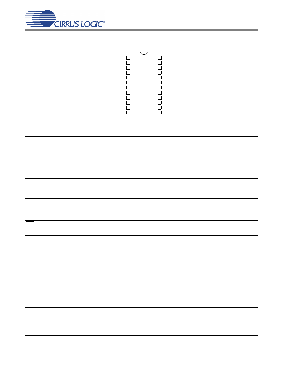
RST
1
24
FILT+
M/S
2
23
REFGND
LRCK
3
22
VQ3
SCLK
4
21
AINR
MCLK
5
20
VQ2
VD
6
19
VA
GND
7
18
GND
VL
8
17
VQ1
SDOUT
9
16
AINL
MDIV
10
15
OVFL
HPF
11
14
M1
I²S/LJ
12
13
M0