Cdb connectors, jumpers, and switches, Table 1. system connections, Table 2. system jumper settings – Cirrus Logic CDB5346 User Manual
Page 9
DS861DB1
9
CDB5346
4. CDB CONNECTORS, JUMPERS, AND SWITCHES
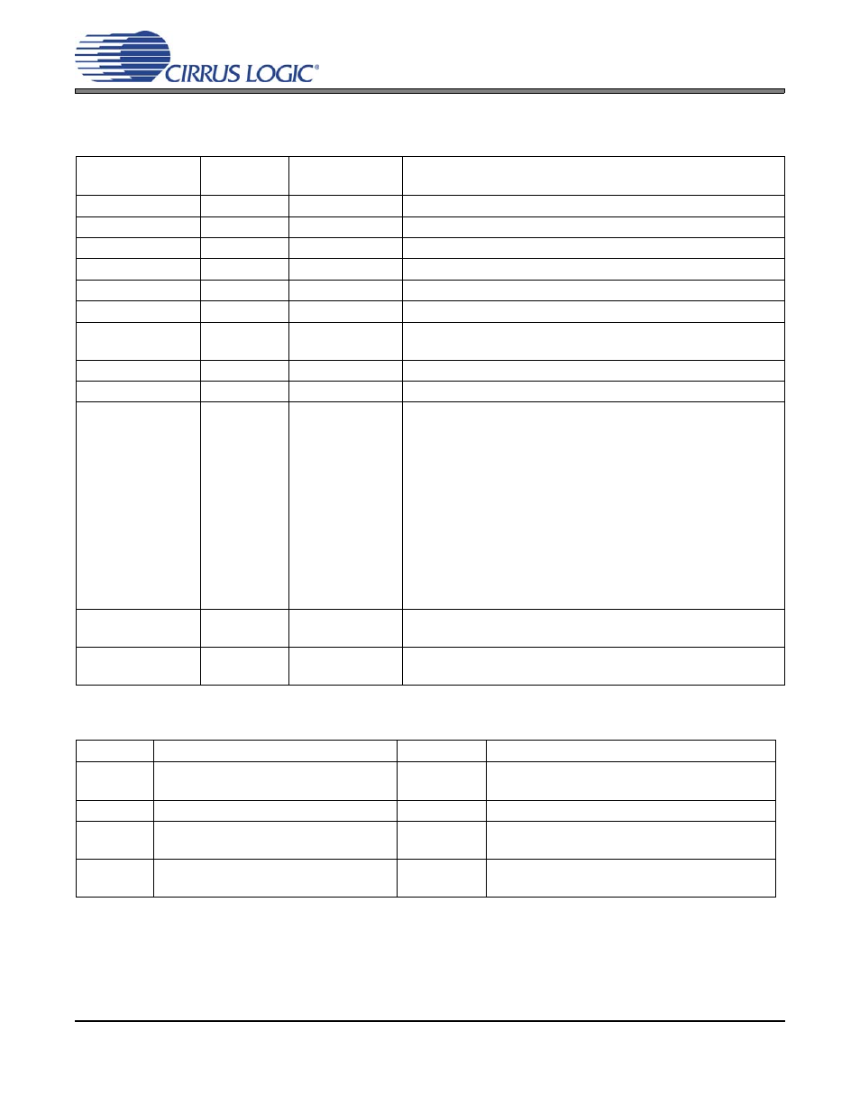
CONNECTOR
Reference
Designator INPUT/OUTPUT
SIGNAL PRESENT
+5V
J22
Input
+5.0 V Power Supply
GND
J24
Input
Ground Reference
S/PDIF TX
J20
Output
CS8406 digital audio output via coaxial cable
S/PDIF TX
OPT1
Output
CS8406 digital audio output via optical cable
USB I/O
J17
Input/Output
USB connection to PC for SPI / I²C control port signals.
PCM I/O
J21
Input/Output
I/O for Serial Audio Clocks & Data
PC / EXTERNAL
CONTROL
J19
Input/Output
I/O for external SPI / I²C control port signals.
C2
J18
Input/Output
I/O for programming the micro controller (U6).
MICRO RESET
S1
Input
Reset for the micro controller (U6).
AIN1A
AIN1B
AIN2A
AIN2B
AIN3A
AIN3B
AIN4A
AIN4B
AIN5A
AIN5B
AIN6A
AIN6B
J1
J2
J3
J4
J5
J6
J7
J8
J9
J10
J11
J12
Input
RCA phono jacks for analog input signal to CS5346. Passive
input filter.
MICIN1
MICIN2
J13
J14
Input
1/8“ TRS jacks for microphone input.
PGA_OUTA
PGA_OUTB
J15
J16
Output
RCA phono jacks for PGA analog outputs. Active output
buffer.
Table 1. System Connections
JUMPER
PURPOSE
POSITION
FUNCTION SELECTED
J27
Selects the source of voltage for the
VLC supply.
+3.3 V
VA*
Voltage source is +3.3 V regulator.
Voltage source is VA.
J25
Disconnect for the VD supply\
+3.3 V*
Voltage source is +3.3 V regulator.
J26
Selects the source of voltage for the
VLS supply.
+3.3 V
VA*
Voltage source is +3.3 V regulator.
Voltage source is VA
J23
Selects the source of voltage for the
VA supply
POST*
USB
Voltage source is +5 V Post
Voltage source is USB bus power.
*Default factory settings
Table 2. System Jumper Settings