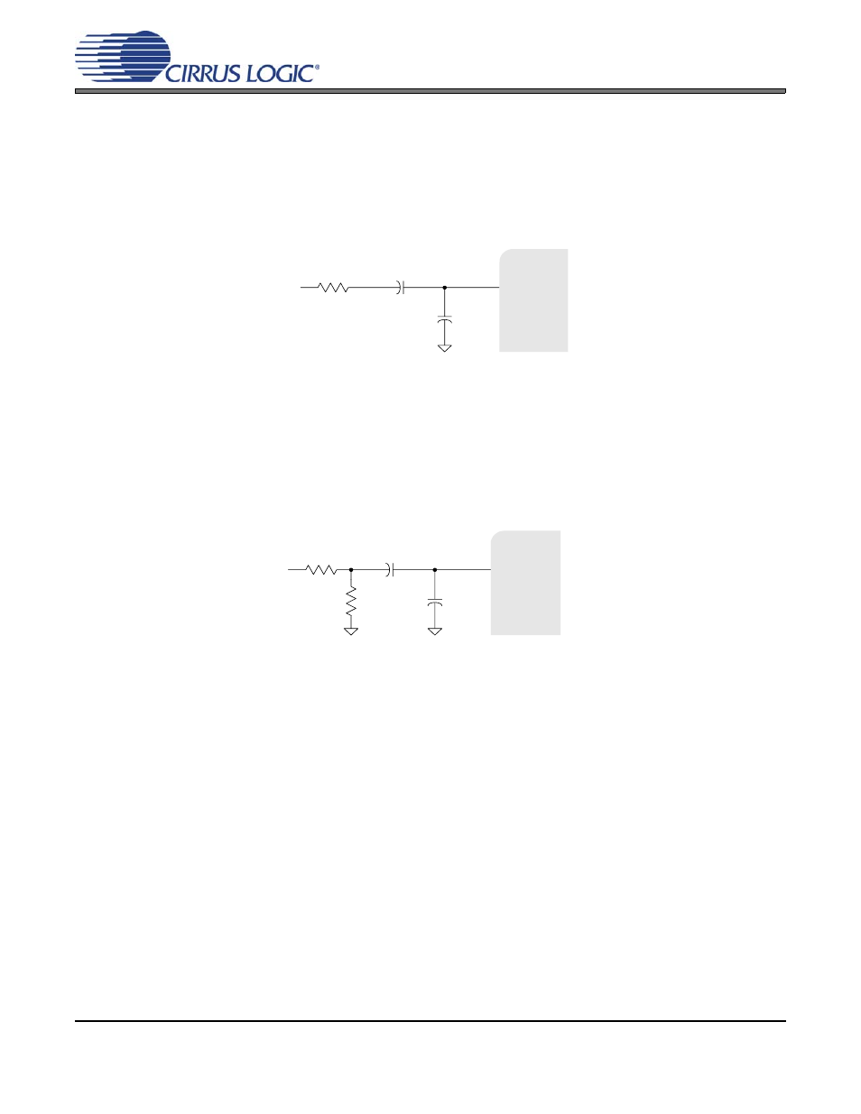
Input filter topology, 1 cs5333 input filter, Figure 3. cs5333 input circuit – Cirrus Logic AN285 User Manual
Page 7: 2 cs5343/4 input filter, 1 cs5343/4 recommended circuit, Figure 4. cs5343/4 typical input circuit, An285 7. input filter topology

AN285REV1
7
AN285
7. INPUT FILTER TOPOLOGY
7.1
CS5333 Input Filter
shows the recommended input circuit for the CS5333. The CS5333 contains an internal continu-
ous-time buffer. The external circuit provides filtering of high-frequency noise via the single-pole RC filter.
The CS5333 will self-bias the input to the reference voltage (half of VA). If the incoming signal is not DC
biased to within 5% of this value, then the series DC-blocking capacitor is necessary.
7.2
CS5343/4 Input Filter
7.2.1
CS5343/4 Recommended Circuit
shows the typical analog input network for the CS5343/4. The component values shown are not
mandatory, but this particular circuit has four features that make it ideal for most applications, as dis-
cussed below. Please see the CS534/4 datasheet for more information regarding component selection.
Figure 4. CS5343/4 Typical Input Circuit
•
Input Impedance: This circuit’s input impedance as seen from the analog source looking into the circuit
is 10 k
Ω, which means this circuit will provide the ideal interface to most consumer equipment.
•
Attenuation: This circuit also attenuates the analog input signal by 6 dB. This further simplifies the in-
terface between consumer equipment and the ADC because most consumer equipment generate 2
Vrms line voltage. The circuit in
attenuates the incoming signal from 2 Vrms to 1 Vrms, which
is the full-scale input voltage of the CS5343/4 when VA = 5V.
•
Source Impedance: The CS5343/4 achieves optimal analog performance when the source impedance
as seen from the ADC looking into this network remains at or below 2.5 k
Ω. The ADC effectively “sees”
two 5 k
Ω resistors in parallel, or 2.5 kΩ!
•
Noise Rejection: Under typical conditions, the modulators in the ADC generate switching noise at
6.144 MHz, or half of the MCLK frequency. The single-pole RC filter formed by the shunt capacitor and
the input impedance of the device will provide approximately 20 dB of attenuation at the modulator
switching frequency. For this and other capacitors in the signal path, capacitors with C0G or other high-
quality dielectric will produce the best results.
C0G
0.47
µF
CS5333
AIN
150
Ω
0.01
µF
Figure 3. CS5333 Input Circuit
270 pF
C0G
1
µF
5k
Ω
CS5343/4
AIN
5k
Ω
