Cirrus Logic CS4397 User Manual
Features, Description
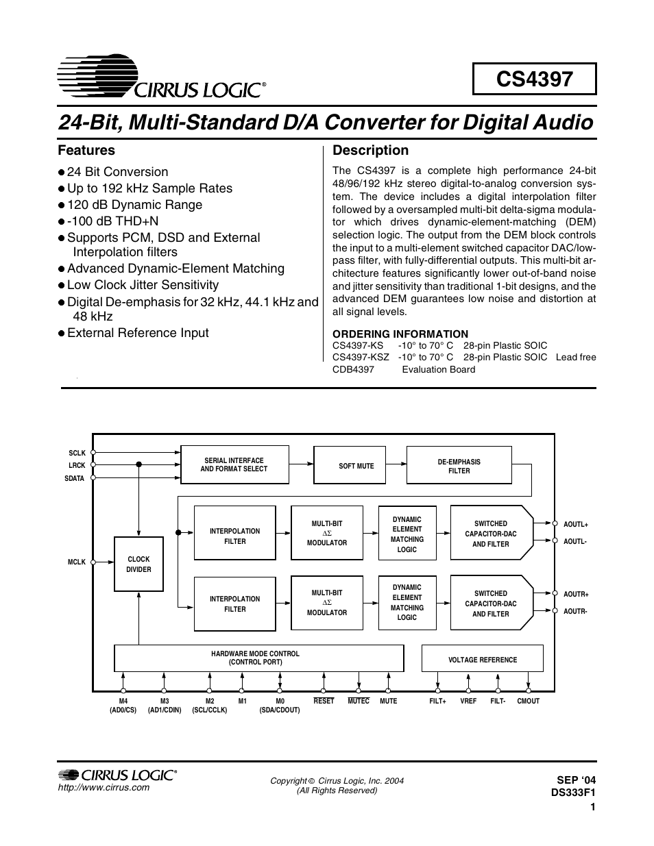
Table of contents
Document Outline
- CS4397
- Features
- Description
- 1.0 Characteristics/Specifications
- ANALOG CHARACTERISTICS
- ANALOG CHARACTERISTICS
- ANALOG CHARACTERISTICS
- ANALOG CHARACTERISTICS - DSD Mode
- ANALOG CHARACTERISTICS - 8x Interpolator Mode
- DIGITAL CHARACTERISTICS
- absolute maximum ratings
- recommended operating conditions
- Switching characteristics
- DSD - Switching characteristics
- 8x Interpolator - Switching characteristics
- SWITCHING CHARACTERISTICS - CONTROL PORT
- SWITCHING CHARACTERISTICS - CONTROL PORT
- 2.0 Typical Connection Diagram
- 3.0 Register Description
- 4.0 PIN DESCRIPTION - PCM mode
- Reset - RST
- Digital Ground - DGND
- Digital Power - VD
- Master Clock - MCLK
- Serial Clock - SCLK
- Left/Right Clock - LRCK
- Serial Audio Data - SDATA
- Soft Mute - MUTE
- Control Port / Hardware Mode Select - C/H
- Mute Control - MUTEC
- Analog Ground - AGND
- Differential Analog Outpus - AOUTR- , AOUTR+ and AOUTL- , AOUTL+
- Analog Power - VA
- Common Mode Voltage - CMOUT
- Reference Ground - FILT-
- Reference Filter - FILT+
- Voltage Reference Input- VREF
- HARDWARE MODE
- Mode Select - M0, M1, M2, M3, M4
- CONTROL PORT MODE
- Address Bit 0 / Chip Select - AD0 / CS
- Address Bit 1 / Control Data Input - AD1/CDIN
- Serial Control Interface Clock - SCL/CCLK
- Serial Control Data I/O - SDA/CDOUT
- M1 - Mode Select
- 5.0 piN DESCRIPTION - DSD mode
- 6.0 piN DESCRIPTION - 8x INterpolator mode
- 7.0 APPLICATIONS
- 8.0 Control Port Interface
- 8.1 SPI Mode
- 8.2 I2C Mode
- Memory Address Pointer (MAP)
- Figure 7. Control Port Timing, SPI mode
- Figure 8. Control Port Timing, I2C Mode
- Table 9. Single Speed (16 to 50kHz) Digital Interface Format Options
- Table 10. Single Speed (16 to 50kHz) De-Emphasis Options
- Table 11. Double Speed (50 to 100 kHz) Sample Rate Mode Options
- Table 12. Quad (100 to 200 kHz) Sample Rate Mode Options
- Table 13. 8x Interpolated Input Mode Options
- Table 14. Direct Stream Digital Options
- Figure 9. Single-speed Transition Band
- Figure 10. Single-speed Stopband Rejection
- Figure 11. Single-speed Transition Band
- Figure 12. Single-speed Frequency Response
- Figure 13. Double-speed Stopband
- Figure 14. Double-speed Transition Band
- Figure 15. Double-speed Transition Band
- Figure 16. Double-speed Frequency Response
- Figure 17. Quad-speed Stopband Rejection
- Figure 18. Quad-speed Transition Band
- Figure 19. Quad-speed Transition Band
- Figure 20. Quad-speed Frequency Response
- Figure 21. 8x Interpolator Stop Band
- Figure 22. 8x Interpolator Transition Band
- Figure 23. 8x Interpolator Transition Band
- Figure 24. 8x Interpolator Frequency Response
- Figure 25. DSD Frequency Response
- Figure 26. DSD Transition Band
- Figure 27. DSD Transition Band
- Figure 28. De-Emphasis Curve
- Figure 29. Format 0, Left Justified
- Figure 30. Format 1, I2S
- Figure 31. Format 2, Right Justified, 16-Bit Data
- Figure 32. Format 3, Right Justified, 24-Bit Data
- Figure 33. Format 4, 8x Interpolator Mode
- Memory Address Pointer (MAP)
- 9.0 PARAMETER DEFINITIONS
- 10.0 REFERENCES
- 11.0 package dimensions