Cirrus Logic CS4397 User Manual
Features, Description
1
Copyright
© Cirrus Logic, Inc. 2004
(All Rights Reserved)
http://www.cirrus.com
CS4397
24-Bit, Multi-Standard D/A Converter for Digital Audio
Features
24 Bit Conversion
Up to 192 kHz Sample Rates
120 dB Dynamic Range
-100 dB THD+N
Supports PCM, DSD and External
Interpolation filters
Advanced Dynamic-Element Matching
Low Clock Jitter Sensitivity
Digital De-emphasis for 32 kHz, 44.1 kHz and
48 kHz
External Reference Input
Description
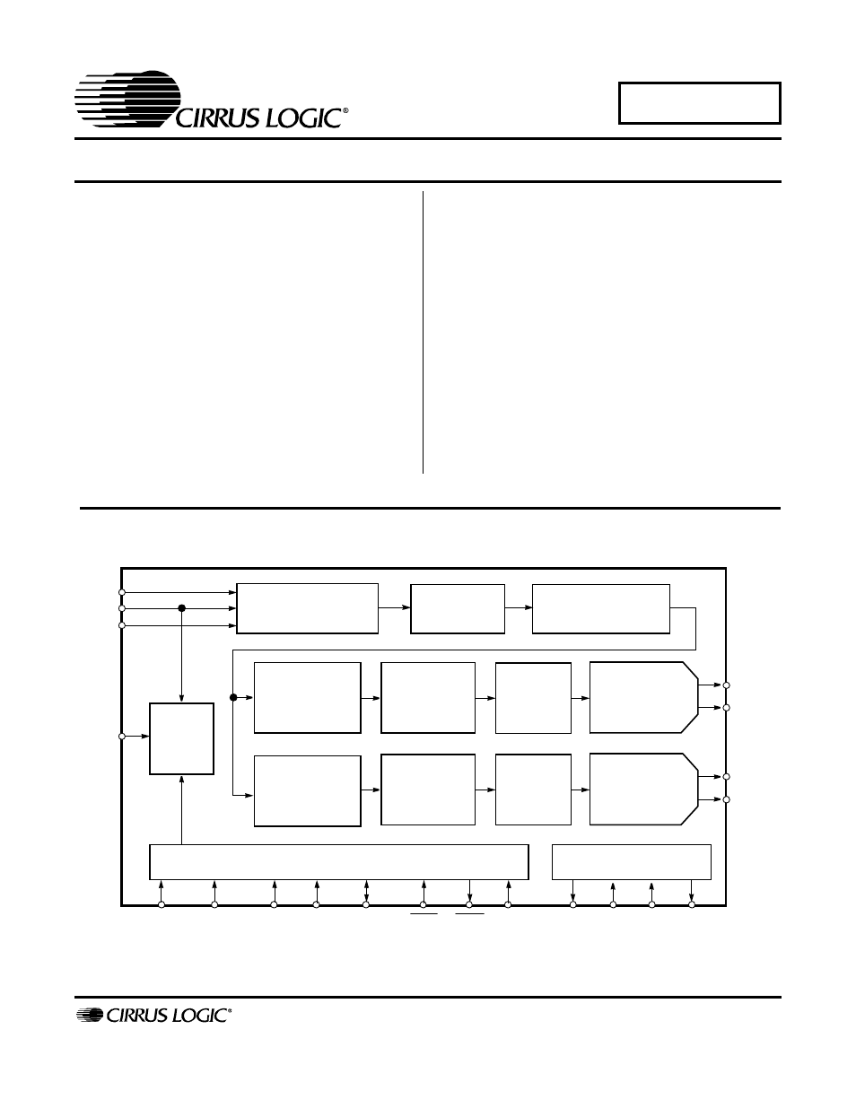
The CS4397 is a complete high performance 24-bit
48/96/192 kHz stereo digital-to-analog conversion sys-
tem. The device includes a digital interpolation filter
followed by a oversampled multi-bit delta-sigma modula-
tor which drives dynamic-element-matching (DEM)
selection logic. The output from the DEM block controls
the input to a multi-element switched capacitor DAC/low-
pass filter, with fully-differential outputs. This multi-bit ar-
chitecture features significantly lower out-of-band noise
and jitter sensitivity than traditional 1-bit designs, and the
advanced DEM guarantees low noise and distortion at
all signal levels.
ORDERING INFORMATION
CS4397-KS
-10° to 70° C
28-pin Plastic SOIC
CS4397-KSZ
-10° to 70° C
28-pin Plastic SOIC Lead free
CDB4397
Evaluation Board
I
SCLK
MCLK
M4
LRCK
SDATA
AOUTL+
AOUTR+
SERIAL INTERFACE
AND FORMAT SELECT
INTERPOLATION
SOFT MUTE
∆Σ
MODULATOR
DYNAMIC
DE-EMPHASIS
SWITCHED
AOUTL-
AOUTR-
FILT+
FILTER
INTERPOLATION
FILTER
FILTER
MULTI-BIT
∆Σ
MODULATOR
MULTI-BIT
ELEMENT
MATCHING
LOGIC
DYNAMIC
ELEMENT
MATCHING
LOGIC
CAPACITOR-DAC
AND FILTER
SWITCHED
CAPACITOR-DAC
AND FILTER
VREF
CMOUT
FILT-
VOLTAGE REFERENCE
HARDWARE MODE CONTROL
CLOCK
DIVIDER
(CONTROL PORT)
(AD0/CS)
M3
M2
(AD1/CDIN)
(SCL/CCLK)
M1
M0
(SDA/CDOUT)
RESET
MUTEC
MUTE
SEP ‘04
DS333F1
Document Outline
- CS4397
- Features
- Description
- 1.0 Characteristics/Specifications
- ANALOG CHARACTERISTICS
- ANALOG CHARACTERISTICS
- ANALOG CHARACTERISTICS
- ANALOG CHARACTERISTICS - DSD Mode
- ANALOG CHARACTERISTICS - 8x Interpolator Mode
- DIGITAL CHARACTERISTICS
- absolute maximum ratings
- recommended operating conditions
- Switching characteristics
- DSD - Switching characteristics
- 8x Interpolator - Switching characteristics
- SWITCHING CHARACTERISTICS - CONTROL PORT
- SWITCHING CHARACTERISTICS - CONTROL PORT
- 2.0 Typical Connection Diagram
- 3.0 Register Description
- 4.0 PIN DESCRIPTION - PCM mode
- Reset - RST
- Digital Ground - DGND
- Digital Power - VD
- Master Clock - MCLK
- Serial Clock - SCLK
- Left/Right Clock - LRCK
- Serial Audio Data - SDATA
- Soft Mute - MUTE
- Control Port / Hardware Mode Select - C/H
- Mute Control - MUTEC
- Analog Ground - AGND
- Differential Analog Outpus - AOUTR- , AOUTR+ and AOUTL- , AOUTL+
- Analog Power - VA
- Common Mode Voltage - CMOUT
- Reference Ground - FILT-
- Reference Filter - FILT+
- Voltage Reference Input- VREF
- HARDWARE MODE
- Mode Select - M0, M1, M2, M3, M4
- CONTROL PORT MODE
- Address Bit 0 / Chip Select - AD0 / CS
- Address Bit 1 / Control Data Input - AD1/CDIN
- Serial Control Interface Clock - SCL/CCLK
- Serial Control Data I/O - SDA/CDOUT
- M1 - Mode Select
- 5.0 piN DESCRIPTION - DSD mode
- 6.0 piN DESCRIPTION - 8x INterpolator mode
- 7.0 APPLICATIONS
- 8.0 Control Port Interface
- 8.1 SPI Mode
- 8.2 I2C Mode
- Memory Address Pointer (MAP)
- Figure 7. Control Port Timing, SPI mode
- Figure 8. Control Port Timing, I2C Mode
- Table 9. Single Speed (16 to 50kHz) Digital Interface Format Options
- Table 10. Single Speed (16 to 50kHz) De-Emphasis Options
- Table 11. Double Speed (50 to 100 kHz) Sample Rate Mode Options
- Table 12. Quad (100 to 200 kHz) Sample Rate Mode Options
- Table 13. 8x Interpolated Input Mode Options
- Table 14. Direct Stream Digital Options
- Figure 9. Single-speed Transition Band
- Figure 10. Single-speed Stopband Rejection
- Figure 11. Single-speed Transition Band
- Figure 12. Single-speed Frequency Response
- Figure 13. Double-speed Stopband
- Figure 14. Double-speed Transition Band
- Figure 15. Double-speed Transition Band
- Figure 16. Double-speed Frequency Response
- Figure 17. Quad-speed Stopband Rejection
- Figure 18. Quad-speed Transition Band
- Figure 19. Quad-speed Transition Band
- Figure 20. Quad-speed Frequency Response
- Figure 21. 8x Interpolator Stop Band
- Figure 22. 8x Interpolator Transition Band
- Figure 23. 8x Interpolator Transition Band
- Figure 24. 8x Interpolator Frequency Response
- Figure 25. DSD Frequency Response
- Figure 26. DSD Transition Band
- Figure 27. DSD Transition Band
- Figure 28. De-Emphasis Curve
- Figure 29. Format 0, Left Justified
- Figure 30. Format 1, I2S
- Figure 31. Format 2, Right Justified, 16-Bit Data
- Figure 32. Format 3, Right Justified, 24-Bit Data
- Figure 33. Format 4, 8x Interpolator Mode
- Memory Address Pointer (MAP)
- 9.0 PARAMETER DEFINITIONS
- 10.0 REFERENCES
- 11.0 package dimensions