Pin description, Pin name # pin description, Cs4384 – Cirrus Logic CS4384 User Manual
Page 6
6
DS620F1
CS4384
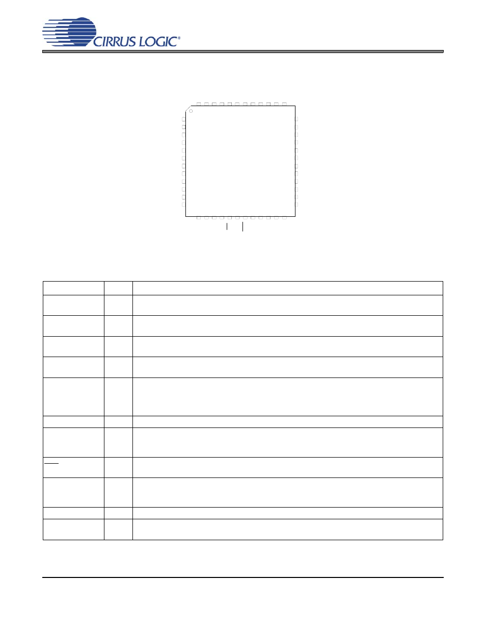
1. PIN DESCRIPTION
Pin Name
#
Pin Description
VD
4
Digital Power (Input) - Positive power supply for the digital section. Refer to the Recommended
Operating Conditions for appropriate voltages.
GND
5
31
Ground (Input) - Ground reference. Should be connected to analog ground.
MCLK
6
Master Clock (Input) - Clock source for the delta-sigma modulator and digital filters.
illus-
trates several standard audio sample rates and the required master clock frequencies.
LRCK
7
Left Right Clock (Input) - Determines which channel, Left or Right, is currently active on the serial
audio data line. The frequency of the left/right clock must be at the audio sample rate, Fs.
SDIN1
SDIN2
SDIN3
SDIN4
8
11
13
14
Serial Data Input (Input) - Input for two’s complement serial audio data.
SCLK
9
Serial Clock (Input) - Serial clocks for the serial audio interface.
VLC
18
Control Port Power (Input) - Determines the required signal level for the control port and hard-
ware mode configuration pins. Refer to the Recommended Operating Conditions for appropriate
voltages.
RST
19
Reset (Input) - The device enters a low power mode and all internal registers are reset to their
default settings when low.
FILT+
20
Positive Voltage Reference (Output) - Positive reference voltage for the internal sampling cir-
cuits. Requires the capacitive decoupling to analog ground as shown in the Typical Connection
Diagram.
VQ
21
Quiescent Voltage (Output) - Filter connection for internal quiescent voltage.
MUTEC1
MUTEC234
41
22
Mute Control (Output) - These pins are intended to be used as a control for external mute circuits
on the line outputs to prevent the clicks and pops that can occur in any single supply system.
SD
IN
3
GND
TST_OUT
AOUT5
TST_OUT
AOUT4
VA
TST_OUT
AOUT6
TST_OUT
AOUT7
6
2
4
8
10
1
3
5
7
9
11
12
13 14 15 16 17 18 19 20 21 22 23 24
31
35
33
29
27
36
34
32
30
28
26
25
48 47 46 45 44 43 42 41 40 39 38 37
MCLK
DSD2
VD
SDIN1
M4(TST)
DSD3
DSD1
GND
SCLK
SDIN2
M3(TST)
LRCK
DS
D
_
S
C
LK
DS
D
6
DS
D
5
DS
D7
CS4384
DS
D8
VLS
SD
IN
4
M2
(SC
L
/C
CL
K)
M1
(S
D
A
/C
DI
N)
VLC
RS
T
FIL
T
+
VQ
MU
TEC2
TST_OUT
AO
UT8
M0(A
D
0
/C
S
)
AOUT3
TST_OUT
AOU
T
2
TST_
O
U
T
TS
T_
OU
T
AO
UT
1
DS
D4
MU
TEC1